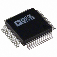
ADUC831BS Analog Devices Inc, ADUC831BS Datasheet - Page 9

ADUC831BS
Manufacturer Part Number
ADUC831BS
Description
IC ADC/DAC 12BIT W/MCU 52-MQFP
Manufacturer
Analog Devices Inc
Series
MicroConverter® ADuC8xxr
Datasheet
1.EVAL-ADUC831QSZ.pdf
(76 pages)
Specifications of ADUC831BS
Rohs Status
RoHS non-compliant
Core Processor
8052
Core Size
8-Bit
Speed
16MHz
Connectivity
EBI/EMI, I²C, SPI, UART/USART
Peripherals
PSM, Temp Sensor, WDT
Number Of I /o
34
Program Memory Size
62KB (62K x 8)
Program Memory Type
FLASH
Eeprom Size
4K x 8
Ram Size
2.25K x 8
Voltage - Supply (vcc/vdd)
2.7 V ~ 5.5 V
Data Converters
A/D 8x12b, D/A 2x12b
Oscillator Type
Internal
Operating Temperature
-40°C ~ 125°C
Package / Case
52-MQFP, 52-PQFP
For Use With
EVAL-ADUC831QSZ - KIT DEV FOR ADUC831 QUICK START
Available stocks
Company
Part Number
Manufacturer
Quantity
Price
Company:
Part Number:
ADUC831BS
Manufacturer:
SHARP
Quantity:
21 512
Company:
Part Number:
ADUC831BS
Manufacturer:
ADI
Quantity:
150
Part Number:
ADUC831BS
Manufacturer:
ADI/亚德诺
Quantity:
20 000
Company:
Part Number:
ADUC831BSB20
Manufacturer:
MINI
Quantity:
892
Company:
Part Number:
ADUC831BSZ
Manufacturer:
Analog Devices Inc
Quantity:
10 000
Part Number:
ADUC831BSZ
Manufacturer:
AD
Quantity:
20 000
Company:
Part Number:
ADUC831BSZ-REEL
Manufacturer:
AD
Quantity:
1 200
Company:
Part Number:
ADUC831BSZ-REEL
Manufacturer:
Analog Devices Inc
Quantity:
10 000
Mnemonic
DV
AV
C
V
AGND
P1.0–P1.7
ADC0–ADC7 I
T2
T2EX
SS
SDATA
SCLOCK
MOSI
MISO
DAC0
DAC1
RESET
P3.0–P3.7
PWMC
PWM0
PWM1
RxD
TxD
INT0
INT1
T0
T1
CONVST
WR
RD
XTAL2
XTAL1
DGND
P2.0–P2.7
(A8–A15)
(A16–A23)
REV. 0
REF
REF
DD
DD
I
I/O
I/O
Type Function
P
P
I
I/O
G
I
I
I
I/O
I/O
I/O
I/O
O
O
I
I
O
O
I/O
O
I
I
I
I
I
O
O
O
I
G
Digital Positive Supply Voltage, 3 V or 5 V Nominal
Analog Positive Supply Voltage, 3 V or 5 V Nominal
Decoupling Input for On-Chip Reference. Connect 0.1 µF between this pin and AGND.
Reference Input/Output. This pin is connected to the internal reference through a series resistor and is the
reference source for the analog-to-digital converter. The nominal internal reference voltage is 2.5 V and this
appears at the pin. This pin can be overdriven by an external reference.
Analog Ground. Ground reference point for the analog circuitry.
Port 1 is an 8-bit input port only. Unlike other ports, Port 1 defaults to Analog Input mode, to configure
any of these Port Pins as a digital input, write a “0” to the port bit. Port 1 pins are multifunction and share
the following functionality.
Analog Inputs. Eight single-ended analog inputs. Channel selection is via ADCCON2 SFR.
Timer 2 Digital Input. Input to Timer/Counter 2. When enabled, Counter 2 is incremented in response to a
1-to-0 transition of the T2 input.
Digital Input. Capture/Reload trigger for Counter 2 and also functions as an Up/Down control input for
Counter 2.
Slave Select Input for the SPI Interface
User Selectable, I
Serial Clock Pin for I
SPI Master Output/Slave Input Data I/O Pin for SPI Interface
SPI Master Input/Slave Output Data I/O Pin for SPI Serial Interface
Voltage Output from DAC0
Voltage Output from DAC1
Digital Input. A high level on this pin for 24 master clock cycles while the oscillator is running resets the device.
Port 3 is a bidirectional port with internal pull-up resistors. Port 3 pins that have 1s written to them are
pulled high by the internal pull-up resistors, and in that state they can be used as inputs. As inputs, Port 3
pins being pulled externally low will source current because of the internal pull-up resistors. Port 3 pins
also contain various secondary functions which are described below.
PWM Clock Input
PWM0 Voltage Output. PWM outputs can be configured to use ports 2.6 and 2.7, or 3.4 and 3.3.
PWM1 Voltage Output. See CFG831 Register for further information.
Receiver Data Input (Asynchronous) or Data Input/Output (Synchronous) of Serial (UART) Port
Transmitter Data Output (Asynchronous) or Clock Output (Synchronous) of Serial (UART) Port
Interrupt 0, programmable edge- or level-triggered Interrupt input, which can be programmed to one of two
priority levels. This pin can also be used as a gate control input to Timer 0.
Interrupt 1, programmable edge- or level-triggered Interrupt input, which can be programmed to one of two
priority levels. This pin can also be used as a gate control input to Timer 1.
Timer/Counter 0 Input
Timer/Counter 1 Input
Active Low Convert Start Logic Input for the ADC Block when the External Convert Start Function is Enabled.
A low-to-high transition on this input puts the track-and-hold into its hold mode and starts conversion.
Write Control Signal, Logic Output. Latches the data byte from Port 0 into the external data memory.
Read Control Signal, Logic Output. Enables the external data memory to Port 0.
Output of the Inverting Oscillator Amplifier
Input to the Inverting Oscillator Amplifier, and input to the internal clock generator circuits.
Digital Ground. Ground reference point for the digital circuitry.
Port 2 is a bidirectional port with internal pull-up resistors. Port 2 pins that have 1s written to them are
pulled high by the internal pull-up resistors, and in that state they can be used as inputs. As inputs, Port 2
pins being pulled externally low will source current because of the internal pull-up resistors. Port 2 emits
the high order address bytes during fetches from external program memory and middle and high order
address bytes during accesses to the external 24-bit external data memory space.
2
C Compatible or SPI Data Input/Output Pin
2
C Compatible or SPI Serial Interface Clock
PIN FUNCTION DESCRIPTIONS
–9–
ADuC831


