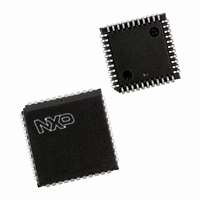
PXAC37KFA/00,512 NXP Semiconductors, PXAC37KFA/00,512 Datasheet - Page 30

PXAC37KFA/00,512
Manufacturer Part Number
PXAC37KFA/00,512
Description
IC XA MCU 16BIT 32K OTP 44-PLCC
Manufacturer
NXP Semiconductors
Series
XAr
Datasheet
1.PXAC37KFA00512.pdf
(68 pages)
Specifications of PXAC37KFA/00,512
Core Processor
XA
Core Size
16-Bit
Speed
32MHz
Connectivity
CAN, EBI/EMI, SPI, UART/USART
Peripherals
DMA, POR, PWM, WDT
Number Of I /o
32
Program Memory Size
32KB (32K x 8)
Program Memory Type
OTP
Ram Size
1K x 8
Voltage - Supply (vcc/vdd)
4.5 V ~ 5.5 V
Oscillator Type
External
Operating Temperature
-40°C ~ 85°C
Package / Case
44-PLCC
Lead Free Status / RoHS Status
Lead free / RoHS Compliant
Eeprom Size
-
Data Converters
-
Other names
568-3533-5
935266516512
PXAC37KFA
935266516512
PXAC37KFA
Available stocks
Company
Part Number
Manufacturer
Quantity
Price
Company:
Part Number:
PXAC37KFA/00,512
Manufacturer:
NXP Semiconductors
Quantity:
10 000
Philips Semiconductors
INPUT/OUTPUT PORT PIN CONFIGURATION
Each I/O port pin can be user–configured to one of four modes:
Quasi–Bidirectional (essentially the same as standard 80C51 family
I/O ports), Open–Drain, Push–Pull, and Off (High Impedance). After
Reset, the default configuration is Quasi–Bidirectional.
I/O port pin configurations are determined by the settings in port
configuration SFRs. There are two SFRs for each port, called
PnCFGA and PnCFGB, where “n” is the port number. One bit in
each of the two SFRs relates to the setting for the corresponding
port pin, allowing any combination of the four modes to be mixed on
any port pins. For instance, the mode of port 1 pin 3 (P1.3) is
controlled by setting bit 3 (P1CFGA[3] and P1CFGB[3]).
Table 13 shows the configuration register settings for the four port
pin modes. The DC electrical characteristics of each mode may be
found in Table 19.
Table 13. Port Configuration Register Settings
Note: Mode changes may cause glitches to occur during transitions.
When modifying both registers, WRITE instructions should be
carried out consecutively.
2000 Jan 25
XA 16-bit microcontroller family
32K/1024 OTP CAN transport layer controller
1 UART, 1 SPI Port, CAN 2.0B, 32 CAN ID filters, transport layer co-processor
PnCFGB
0
0
1
1
PnCFGA
0
1
0
1
Figure 18. UART Multiprocessor Communication, Automatic Address Recognition
START
BIT
IN UART MODE 2 OR MODE 3 AND SM2_0 = 1:
– WHEN OWN ADDRESS RECEIVED, CLEAR SM2_0 TO RECEIVE DATA BYTES
– WHEN ALL DATA BYTES HAVE BEEN RECEIVED: SET SM2_0 TO WAIT FOR NEXT ADDRESS.
D0
INTERRUPT IF REN_0=1, RB8_0=1 AND “RECEIVED ADDRESS” = “PROGRAMMED ADDRESS”
Open–Drain
Quasi–Bidirectional
Off (High Impedance)
Push–Pull
RECEIVED ADDRESS D0 TO D7
—
PROGRAMMED ADDRESS
D0
Port Pin Mode
D1
—
D1
Figure 17. UART Framing Error Detection
D2
SM0_0
—
D2
1
1
D3
SM1_0
D3
DATA BYTE
—
1
0
D4
23
FE0
SM2_0
D4
EXTERNAL BUS
If off chip code is selected (through the use of the EA/ pin), initial
code fetches will be done within a full 20–bit address space. The
External PROGRAM/DATA bus provides 16 bit width in a 20–bit
ADDRESS space.
RESET
Refer to Figure 19 for a recommended Reset circuit example.
COMPARATOR
SOME TYPICAL VALUES FOR R AND C:
(ASSUMING THAT THE V
D5
1
R = 100K, C = 1.0 F
R = 1.0M, C = 0.1 F
D5
REN_0
BR0
1
D6
Figure 19. Recommended Reset Circuit
D6
TB8_0
OE0
C
D7
X
R
V
DD
DD
RISE TIME IS 1ms OR LESS)
D7
STINT0
RB8_0
D8
MODE 2, 3
ONLY IN
RESET
D8
S0STAT
TI_0
XA
if 0, sets FE
STOP
BIT
Preliminary specification
RI_0
SU01331
SU01332
S0CON
XA-C3
SU00702


