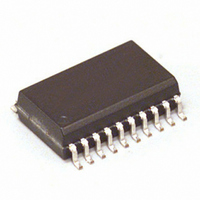
MC68HC908JK3CDW Freescale Semiconductor, MC68HC908JK3CDW Datasheet - Page 135

MC68HC908JK3CDW
Manufacturer Part Number
MC68HC908JK3CDW
Description
IC MCU 8MHZ 4K FLASH 20-SOIC
Manufacturer
Freescale Semiconductor
Series
HC08r
Datasheet
1.MC68HC908JK1CDW.pdf
(212 pages)
Specifications of MC68HC908JK3CDW
Core Processor
HC08
Core Size
8-Bit
Speed
8MHz
Peripherals
LED, LVD, POR, PWM
Number Of I /o
15
Program Memory Size
4KB (4K x 8)
Program Memory Type
FLASH
Ram Size
128 x 8
Voltage - Supply (vcc/vdd)
2.7 V ~ 3.3 V
Data Converters
A/D 12x8b
Oscillator Type
External
Operating Temperature
-40°C ~ 85°C
Package / Case
20-SOIC (7.5mm Width)
Lead Free Status / RoHS Status
Contains lead / RoHS non-compliant
Eeprom Size
-
Connectivity
-
- Current page: 135 of 212
- Download datasheet (3Mb)
MC68H(R)C908JL3
Freescale Semiconductor
NOTE:
—
Rev. 1.1
MSxB — Mode Select Bit B
MSxA — Mode Select Bit A
Before changing a channel function by writing to the MSxB or MSxA bit,
set the TSTOP and TRST bits in the TIM status and control register
(TSC).
ELSxB and ELSxA — Edge/Level Select Bits
This read/write bit selects buffered output compare/PWM operation.
MSxB exists only in the TIM channel 0 status and control register.
Setting MS0B disables the channel 1 status and control register and
reverts TCH1 to general-purpose I/O.
Reset clears the MSxB bit.
When ELSxB:A ≠ 00, this read/write bit selects either input capture
operation or unbuffered output compare/PWM operation.
See
When ELSxB:A = 00, this read/write bit selects the initial output level
of the TCHx pin. (See
When channel x is an input capture channel, these read/write bits
control the active edge-sensing logic on channel x.
When channel x is an output compare channel, ELSxB and ELSxA
control the channel x output behavior when an output compare
occurs.
When ELSxB and ELSxA are both clear, channel x is not connected
to an I/O port, and pin TCHx is available as a general-purpose I/O pin.
Table 10-3
ELSxB and ELSxA bits.
1 = Buffered output compare/PWM operation enabled
0 = Buffered output compare/PWM operation disabled
1 = Unbuffered output compare/PWM operation
0 = Input capture operation
1 = Initial output level low
0 = Initial output level high
Table
Timer Interface Module (TIM)
10-3.
shows how ELSxB and ELSxA work. Reset clears the
Table
10-3.) Reset clears the MSxA bit.
Timer Interface Module (TIM)
Technical Data
133
Related parts for MC68HC908JK3CDW
Image
Part Number
Description
Manufacturer
Datasheet
Request
R
Part Number:
Description:
Manufacturer:
Freescale Semiconductor, Inc
Datasheet:
Part Number:
Description:
Manufacturer:
Freescale Semiconductor, Inc
Datasheet:
Part Number:
Description:
Manufacturer:
Freescale Semiconductor, Inc
Datasheet:
Part Number:
Description:
Manufacturer:
Freescale Semiconductor, Inc
Datasheet:
Part Number:
Description:
Manufacturer:
Freescale Semiconductor, Inc
Datasheet:
Part Number:
Description:
Manufacturer:
Freescale Semiconductor, Inc
Datasheet:
Part Number:
Description:
Manufacturer:
Freescale Semiconductor, Inc
Datasheet:
Part Number:
Description:
Manufacturer:
Freescale Semiconductor, Inc
Datasheet:
Part Number:
Description:
Manufacturer:
Freescale Semiconductor, Inc
Datasheet:
Part Number:
Description:
Manufacturer:
Freescale Semiconductor, Inc
Datasheet:
Part Number:
Description:
Manufacturer:
Freescale Semiconductor, Inc
Datasheet:
Part Number:
Description:
Manufacturer:
Freescale Semiconductor, Inc
Datasheet:
Part Number:
Description:
Manufacturer:
Freescale Semiconductor, Inc
Datasheet:
Part Number:
Description:
Manufacturer:
Freescale Semiconductor, Inc
Datasheet:
Part Number:
Description:
Manufacturer:
Freescale Semiconductor, Inc
Datasheet:


