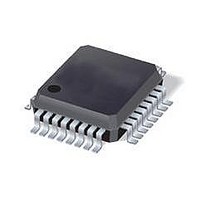
C8051F017 Silicon Laboratories Inc, C8051F017 Datasheet - Page 104

C8051F017
Manufacturer Part Number
C8051F017
Description
IC 8051 MCU 32K FLASH 32LQFP
Manufacturer
Silicon Laboratories Inc
Series
C8051F01xr
Specifications of C8051F017
Core Processor
8051
Core Size
8-Bit
Speed
25MHz
Connectivity
SMBus (2-Wire/I²C), SPI, UART/USART
Peripherals
Brown-out Detect/Reset, POR, PWM, Temp Sensor, WDT
Number Of I /o
8
Program Memory Size
32KB (32K x 8)
Program Memory Type
FLASH
Ram Size
2.25K x 8
Voltage - Supply (vcc/vdd)
2.7 V ~ 3.6 V
Data Converters
A/D 4x10b; D/A 2x12b
Oscillator Type
Internal
Operating Temperature
-40°C ~ 85°C
Package / Case
32-LQFP
Data Bus Width
8 bit
Data Ram Size
2.25 KB
Interface Type
SMBus, SPI, UART
Maximum Clock Frequency
25 MHz
Number Of Programmable I/os
8
Number Of Timers
16 bit
Operating Supply Voltage
2.7 V to 3.6 V
Maximum Operating Temperature
+ 85 C
Mounting Style
SMD/SMT
Minimum Operating Temperature
- 40 C
On-chip Adc
10 bit, 4 Channel
On-chip Dac
12 bit, 2 Channel
Lead Free Status / RoHS Status
Contains lead / RoHS non-compliant
Eeprom Size
-
Lead Free Status / Rohs Status
No
Available stocks
Company
Part Number
Manufacturer
Quantity
Price
Company:
Part Number:
C8051F017
Manufacturer:
Silicon Laboratories Inc
Quantity:
10 000
Company:
Part Number:
C8051F017-GQ
Manufacturer:
Silicon Labs
Quantity:
135
Company:
Part Number:
C8051F017-GQ
Manufacturer:
Silicon Laboratories Inc
Quantity:
10 000
Company:
Part Number:
C8051F017-GQR
Manufacturer:
Silicon Laboratories Inc
Quantity:
10 000
Company:
Part Number:
C8051F017R
Manufacturer:
Silicon Laboratories Inc
Quantity:
10 000
not affect the push-pull Port I/O. Furthermore, the weak pullup is turned off on an open-drain output that is driving
a 0 to avoid unnecessary power dissipation.
The third and final step is to initialize the individual resources selected using the appropriate setup registers.
Initialization procedures for the various digital resources may be found in the detailed explanation of each available
function. The reset state of each register is shown in the figures that describe each individual register.
Highest
Lowest
Priority
Priority
Latches
Port
WEAKPUD
PUSH-PULL
/PORT-OUTENABLE
PORT-OUTPUT
PORT-INPUT
T0, T1, T2,
T2EX,
/INT0,
/INT1
/SYSCLK
CNVSTR
Comptr.
Outputs
SMBus
UART
P0
P1
P2
P3
PCA
SPI
(P0.0-P0.7)
(P1.0-P1.7)
(P2.0-P2.7)
(P3.0-P3.7)
Figure 15.1. Port I/O Functional Block Diagram
8
8
8
8
2
4
2
6
2
6
Figure 15.2. Port I/O Cell Block Diagram
XBR2 Registers
XBR0, XBR1,
Rev. 1.7
Crossbar
Decoder
Priority
Digital
VDD
8
8
8
PRT0CF, PRT1CF,
PRT2CF Registers
PRT3CF
Register
DGND
Cells
Cells
Cells
Cells
VDD
I/O
I/O
I/O
I/O
P0
P1
P2
P3
C8051F000/1/2/5/6/7
C8051F010/1/2/5/6/7
VDD
(WEAK)
External
Pins
P0.0
P0.7
P1.0
P1.7
P2.0
P2.7
P3.0
P3.7
PORT
PAD
Highest
Priority
Lowest
Priority
104


