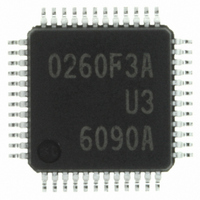
M30260F3AGP#U3 Renesas Electronics America, M30260F3AGP#U3 Datasheet - Page 193

M30260F3AGP#U3
Manufacturer Part Number
M30260F3AGP#U3
Description
IC M16C/TINY MCU FLASH 48LQFP
Manufacturer
Renesas Electronics America
Series
M16C™ M16C/Tiny/26r
Specifications of M30260F3AGP#U3
Core Processor
M16C/60
Core Size
16-Bit
Speed
20MHz
Connectivity
I²C, IEBus, SIO, UART/USART
Peripherals
DMA, PWM, Voltage Detect, WDT
Number Of I /o
39
Program Memory Size
24KB (24K x 8)
Program Memory Type
FLASH
Ram Size
1K x 8
Voltage - Supply (vcc/vdd)
2.7 V ~ 5.5 V
Data Converters
A/D 12x10b
Oscillator Type
Internal
Operating Temperature
-40°C ~ 85°C
Package / Case
48-LQFP
Lead Free Status / RoHS Status
Lead free / RoHS Compliant
Eeprom Size
-
Available stocks
Company
Part Number
Manufacturer
Quantity
Price
- Current page: 193 of 354
- Download datasheet (4Mb)
R
R
M
e
E
1
. v
J
Figure 13.1.5.1. Bus Collision Detect Function-Related Bits
6
0
2
C
9
0 .
B
2 /
Transfer clock
Transfer clock
NOTES:
RxD2
This diagram applies to the case where the IOPOL is set to "1" (reversed)
TxD2
RxD2
Timer A0
TxD2
TxD2
TxD2
RxD2
BCNIC register
IR bit
U2C1 register
TE bit
CLK2
Transfer clock
0
0
(3) The SSS bit in the U2SMR register (Transmit start condition select)
(1) The ABSCS bit in the U2SMR register (bus collision detect sampling clock select)
(2) The ACSE bit in the U2SMR register (auto clear of transmit enable bit)
6
2
1. The falling edge of RxD2 when the IOPOL is set to "0"; the rising edge of RxD2 when the IOPOL is set to "1".
2. The transmit condition must be met before the falling edge (Note 1) of RxD.
0
A
F
2
e
If SSS bit is set to "0", the serial I/O starts sending data one transfer clock cycle after the transmission enable condition is met.
If SSS bit = 1, the serial I/O starts sending data at the rising edge
G
0 -
b
(1)
1 .
o r
2
0
, 5
u
0
p
2
0
(
M
0
Transmission enable condition is met
7
1
6
C
page 174
2 /
6
, A
(2)
If ABSCS=0, bus collision is determined at the rising edge of the transfer clock
M
1
f o
6
ST
ST
3
C
Input to TA0
2
2 /
9
6
, B
ST
ST
D0
D0
M
1
6
D0
D0
IN
C
D1
D1
2 /
6
) T
D1
D1
.
D2
D2
A0 (one-shot timer mode) underflows
If ABSCS is set to "1", bus collision is determined when timer
D2
D2
D3
D3
(1)
D3
D3
of RxD2
D4
D4
D4
D4
D5
D5
D5
D5
D6
D6
D6
D6
If ACSE bit is set to "1"
automatically clear when bus collision
occurs), the TE bit is cleared to "0"
(transmission disabled) when
the IR bit in the BCNIC register is
set to "1" (unmatching detected).
D7
D7
D7
D7
D8
D8
D8
.
D8
SP
SP
SP
SP
13. Serial I/O
Related parts for M30260F3AGP#U3
Image
Part Number
Description
Manufacturer
Datasheet
Request
R

Part Number:
Description:
KIT STARTER FOR M16C/29
Manufacturer:
Renesas Electronics America
Datasheet:

Part Number:
Description:
KIT STARTER FOR R8C/2D
Manufacturer:
Renesas Electronics America
Datasheet:

Part Number:
Description:
R0K33062P STARTER KIT
Manufacturer:
Renesas Electronics America
Datasheet:

Part Number:
Description:
KIT STARTER FOR R8C/23 E8A
Manufacturer:
Renesas Electronics America
Datasheet:

Part Number:
Description:
KIT STARTER FOR R8C/25
Manufacturer:
Renesas Electronics America
Datasheet:

Part Number:
Description:
KIT STARTER H8S2456 SHARPE DSPLY
Manufacturer:
Renesas Electronics America
Datasheet:

Part Number:
Description:
KIT STARTER FOR R8C38C
Manufacturer:
Renesas Electronics America
Datasheet:

Part Number:
Description:
KIT STARTER FOR R8C35C
Manufacturer:
Renesas Electronics America
Datasheet:

Part Number:
Description:
KIT STARTER FOR R8CL3AC+LCD APPS
Manufacturer:
Renesas Electronics America
Datasheet:

Part Number:
Description:
KIT STARTER FOR RX610
Manufacturer:
Renesas Electronics America
Datasheet:

Part Number:
Description:
KIT STARTER FOR R32C/118
Manufacturer:
Renesas Electronics America
Datasheet:

Part Number:
Description:
KIT DEV RSK-R8C/26-29
Manufacturer:
Renesas Electronics America
Datasheet:

Part Number:
Description:
KIT STARTER FOR SH7124
Manufacturer:
Renesas Electronics America
Datasheet:

Part Number:
Description:
KIT STARTER FOR H8SX/1622
Manufacturer:
Renesas Electronics America
Datasheet:

Part Number:
Description:
KIT DEV FOR SH7203
Manufacturer:
Renesas Electronics America
Datasheet:


