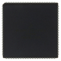
MC68HC11K1CFNE4 Freescale Semiconductor, MC68HC11K1CFNE4 Datasheet - Page 171

MC68HC11K1CFNE4
Manufacturer Part Number
MC68HC11K1CFNE4
Description
IC MCU 640EEPROM 4MHZ 84-PLCC
Manufacturer
Freescale Semiconductor
Series
HC11r
Specifications of MC68HC11K1CFNE4
Core Processor
HC11
Core Size
8-Bit
Speed
4MHz
Connectivity
SCI, SPI
Peripherals
POR, PWM, WDT
Number Of I /o
37
Program Memory Type
ROMless
Eeprom Size
640 x 8
Ram Size
768 x 8
Voltage - Supply (vcc/vdd)
4.5 V ~ 5.5 V
Data Converters
A/D 8x8b
Oscillator Type
Internal
Operating Temperature
-40°C ~ 85°C
Package / Case
84-PLCC
Data Bus Width
8 bit
Data Ram Size
768 B
Interface Type
SCI, SPI
Maximum Clock Frequency
4 MHz
Number Of Programmable I/os
37
Number Of Timers
8
Maximum Operating Temperature
+ 85 C
Mounting Style
SMD/SMT
Minimum Operating Temperature
- 40 C
On-chip Adc
8 bit, 8 Channel
Lead Free Status / RoHS Status
Lead free / RoHS Compliant
Program Memory Size
-
Lead Free Status / Rohs Status
Details
Available stocks
Company
Part Number
Manufacturer
Quantity
Price
Company:
Part Number:
MC68HC11K1CFNE4
Manufacturer:
MOTOROL
Quantity:
115
Company:
Part Number:
MC68HC11K1CFNE4
Manufacturer:
Freescale Semiconductor
Quantity:
10 000
Part Number:
MC68HC11K1CFNE4
Manufacturer:
FREESCALE
Quantity:
20 000
Company:
Part Number:
MC68HC11K1CFNE4R
Manufacturer:
Freescale Semiconductor
Quantity:
10 000
- Current page: 171 of 290
- Download datasheet (4Mb)
8.4.4 Slave Select (SS)
8.4.5 SPI Timing
M68HC11K Family
MOTOROLA
(CPHA = 0) DATA OUT
(CPHA = 1) DATA OUT
FOR REFERENCE
SCK (CPOL = 0)
SCK (CPOL = 1)
SAMPLE INPUT
SAMPLE INPUT
SS (TO SLAVE)
SCK CYCLE #
The slave select (SS) input is used to target specific devices in the SPI
system. It must be pulled low on a targeted slave device prior to any
communication with a master and must remain low for the duration of the
transaction. SS must always be high on any device in master mode.
Pulling SS low on a master mode device generates a mode fault error
(see
Four possible timing relationships are available through control bits
CPOL (clock polarity) and CPHA (clock phase) in the SPCR. These bits
must be the same in both master and slave devices. The master device
always places data on the MOSI line approximately a half-cycle before
the SCK clock edge. This enables the slave device to latch the data. See
Figure
A write collision is normally a slave error because a slave has no control
over when a master initiates a transfer. A master knows when a transfer
is in progress, so there is no reason for a master to generate a
write-collision error, although the SPI logic can detect write collisions in
both master and slave devices.
MSB
Freescale Semiconductor, Inc.
Figure 8-2. Data Clock Timing Diagram
For More Information On This Product,
8.5.1 Mode Fault
MSB
1
8-2.
6
Serial Peripheral Interface (SPI)
Go to: www.freescale.com
2
6
5
3
5
4
Error).
4
4
3
5
3
2
6
2
1
Serial Peripheral Interface (SPI)
7
1
LSB
SPI Signal Descriptions
LSB
8
Technical Data
171
Related parts for MC68HC11K1CFNE4
Image
Part Number
Description
Manufacturer
Datasheet
Request
R

Part Number:
Description:
MC68HC11 EEPROM Programming from a Personal Computer
Manufacturer:
Motorola / Freescale Semiconductor
Part Number:
Description:
Manufacturer:
Freescale Semiconductor, Inc
Datasheet:
Part Number:
Description:
Manufacturer:
Freescale Semiconductor, Inc
Datasheet:
Part Number:
Description:
Manufacturer:
Freescale Semiconductor, Inc
Datasheet:
Part Number:
Description:
Manufacturer:
Freescale Semiconductor, Inc
Datasheet:
Part Number:
Description:
Manufacturer:
Freescale Semiconductor, Inc
Datasheet:
Part Number:
Description:
Manufacturer:
Freescale Semiconductor, Inc
Datasheet:
Part Number:
Description:
Manufacturer:
Freescale Semiconductor, Inc
Datasheet:
Part Number:
Description:
Manufacturer:
Freescale Semiconductor, Inc
Datasheet:
Part Number:
Description:
Manufacturer:
Freescale Semiconductor, Inc
Datasheet:
Part Number:
Description:
Manufacturer:
Freescale Semiconductor, Inc
Datasheet:
Part Number:
Description:
Manufacturer:
Freescale Semiconductor, Inc
Datasheet:
Part Number:
Description:
Manufacturer:
Freescale Semiconductor, Inc
Datasheet:
Part Number:
Description:
Manufacturer:
Freescale Semiconductor, Inc
Datasheet:
Part Number:
Description:
Manufacturer:
Freescale Semiconductor, Inc
Datasheet:


