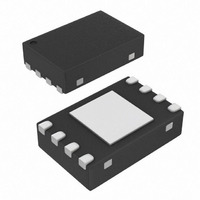
MCP6V01T-E/MNY Microchip Technology, MCP6V01T-E/MNY Datasheet - Page 7

MCP6V01T-E/MNY
Manufacturer Part Number
MCP6V01T-E/MNY
Description
IC OPAMP AUTO-ZERO SGL 8-TDFN
Manufacturer
Microchip Technology
Datasheet
1.MCP6V01RD-TCPL.pdf
(44 pages)
Specifications of MCP6V01T-E/MNY
Slew Rate
0.5 V/µs
Package / Case
8-TDFN
Amplifier Type
Chopper (Zero-Drift)
Number Of Circuits
1
Output Type
Rail-to-Rail
Gain Bandwidth Product
1.3MHz
Current - Input Bias
1pA
Voltage - Input Offset
2µV
Current - Supply
300µA
Current - Output / Channel
22mA
Voltage - Supply, Single/dual (±)
1.8 V ~ 5.5 V
Operating Temperature
-40°C ~ 125°C
Mounting Type
Surface Mount
Number Of Channels
1
Common Mode Rejection Ratio (min)
130 dB
Input Offset Voltage
0.002 mV
Input Bias Current (max)
1 pA
Operating Supply Voltage
3 V, 5 V
Maximum Operating Temperature
+ 125 C
Minimum Operating Temperature
- 40 C
Mounting Style
SMD/SMT
Shutdown
No
Supply Voltage (max)
5.5 V
Supply Voltage (min)
1.8 V
Technology
CMOS
Voltage Gain Db
156 dB
Lead Free Status / RoHS Status
Lead free / RoHS Compliant
For Use With
MCP6V01DM-VOS - DEMO BOARD FOR MCP6V01MCP6V01RD-TCPL - REF DESIGN THERMCPL FOR MCP6V01
-3db Bandwidth
-
Lead Free Status / Rohs Status
Lead free / RoHS Compliant
Other names
MCP6V01T-E/MNYTR
Available stocks
Company
Part Number
Manufacturer
Quantity
Price
Company:
Part Number:
MCP6V01T-E/MNY
Manufacturer:
Renesas
Quantity:
91
Part Number:
MCP6V01T-E/MNY
Manufacturer:
MICROCHIP/微芯
Quantity:
20 000
2.0
Note: Unless otherwise indicated, T
V
2.1
FIGURE 2-1:
FIGURE 2-2:
FIGURE 2-3:
Quadratic Temp Co.
© 2008 Microchip Technology Inc.
L
Note:
= V
22%
20%
18%
16%
14%
12%
10%
22%
20%
18%
16%
14%
12%
10%
8%
6%
4%
2%
0%
8%
6%
4%
2%
0%
DD
20%
18%
16%
14%
12%
10%
8%
6%
4%
2%
0%
TYPICAL PERFORMANCE CURVES
DC Input Precision
/2, R
78 Samples
V
Soldered on PCB
78 Samples
V
Soldered on PCB
DD
DD
The graphs and tables provided following this note are a statistical summary based on a limited number of
samples and are provided for informational purposes only. The performance characteristics listed herein
are not tested or guaranteed. In some graphs or tables, the data presented may be outside the specified
operating range (e.g., outside specified power supply range) and therefore outside the warranted range.
78 Samples
T
V
Soldered on PCB
Input Offset Voltage's Quadratic Temp Co;
= 1.8V and 5.5V
= 1.8V and 5.5V
A
DD
L
= +25°C
Input Offset Voltage Drift; TC
= 1.8V and 5.5V
= 20 kΩ to V
Input Offset Voltage (µV)
Input Offset Voltage.
Input Offset Voltage Drift.
Input Offset Voltage
TC
2
L
(nV/°C
, C
L
= 60 pF, and CS = GND.
2
)
A
= +25°C, V
1
(nV/°C)
DD
= +1.8V to 5.5V, V
FIGURE 2-4:
Power Supply Voltage with V
FIGURE 2-5:
Power Supply Voltage with V
FIGURE 2-6:
Output Voltage.
-1
-2
-3
-4
-1
-2
-3
-4
-1
-2
-3
-4
4
3
2
1
0
4
3
2
1
0
4
3
2
1
0
0.0 0.5 1.0 1.5 2.0 2.5 3.0 3.5 4.0 4.5 5.0 5.5 6.0 6.5
0.0 0.5 1.0 1.5 2.0 2.5 3.0 3.5 4.0 4.5 5.0 5.5 6.0 6.5
0.0 0.5 1.0 1.5 2.0 2.5 3.0 3.5 4.0 4.5 5.0 5.5
SS
= GND, V
V
DD
= 1.8V
Representative Part
Power Supply Voltage (V)
Power Supply Voltage (V)
CM
MCP6V01/2/3
Output Voltage (V)
Input Offset Voltage vs.
Input Offset Voltage vs.
Input Offset Voltage vs.
= V
+125°C
+85°C
+25°C
-40°C
DD
+125°C
+85°C
+25°C
-40°C
/3, V
CM
CM
OUT
V
DD
= V
= V
= 5.5V
V
Representative Part
V
Representative Part
DS22058C-page 7
CM
CM
= V
= V
CMR_L
= V
CMR_H
DD
CMR_L
CMR_H
/2,
.
.


