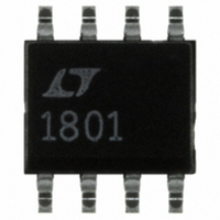
LT1801CS8#PBF Linear Technology, LT1801CS8#PBF Datasheet

LT1801CS8#PBF
Specifications of LT1801CS8#PBF
Available stocks
Related parts for LT1801CS8#PBF
LT1801CS8#PBF Summary of contents
Page 1
... Driving A/D Converters n Rail-to-Rail Buffer Amplifi ers n Active Filters n Video Line Driver L, LT, LTC and LTM are registered trademarks of Linear Technology Corporation. All other trademarks are the property of their respective owners. TYPICAL APPLICATION 3V, 1MHz, 4th Order Butterworth Filter 909Ω 47pF 1.1k 909Ω ...
Page 2
... LEAD FREE FINISH TAPE AND REEL LT1801CDD#PBF LT1801CDD#TRPBF LT1801IDD#PBF LT1801IDD#TRPBF LT1801CMS8#PBF LT1801CMS8#TRPBF LT1801IMS8#PBF LT1801IMS8#TRPBF LT1801CS8#PBF LT1801CS8#TRPBF LT1801IS8#PBF LT1801IS8#TRPBF LT1802CS#PBF LT1802CS#TRPBF LT1802IS#PBF LT1802IS#TRPBF Consult LTC Marketing for parts specifi ed with wider operating temperature ranges. *The temperature grade is identifi label on the shipping container. ...
Page 3
ELECTRICAL CHARACTERISTICS T = 25° 5V, 0V 3V, 0V SYMBOL PARAMETER V Input Offset Voltage OS ΔV Input Offset Shift OS Input Offset Voltage Match (Channel-to-Channel) (Note 9) I Input Bias ...
Page 4
LT1801/LT1802 ELECTRICAL CHARACTERISTICS of 0°C < T < 70° 5V, 0V 3V, 0V SYMBOL PARAMETER V Input Offset Voltage OS ΔV Input Offset Shift OS Input Offset Voltage Match (Channel-to-Channel) (Note 9) ...
Page 5
ELECTRICAL CHARACTERISTICS of – 40°C < T < 85° 5V, 0V 3V, 0V SYMBOL PARAMETER V Input Offset Voltage OS ΔV Input Offset Shift OS Input Offset Voltage Match (Channel-to-Channel) (Note 9) ...
Page 6
LT1801/LT1802 ELECTRICAL CHARACTERISTICS SYMBOL PARAMETER V Input Offset Voltage OS ΔV Input Offset Shift OS Input Offset Voltage Match (Channel-to-Channel) (Note 9) I Input Bias Current B Input Bias Current Match (Channel-to-Channel) (Note 9) I Input Offset Current OS Input ...
Page 7
ELECTRICAL CHARACTERISTICS of 0°C < T < 70° ± SYMBOL PARAMETER V Input Offset Voltage OS ΔV Input Offset Shift OS Input Offset Voltage Match (Channel-to-Channel) (Note ...
Page 8
LT1801/LT1802 ELECTRICAL CHARACTERISTICS of – 40°C < T < 85° ±5V 0V SYMBOL PARAMETER V TC Input Offset Voltage Drift (Note Input Bias Current B Input Bias Current Match ...
Page 9
TYPICAL PERFORMANCE CHARACTERISTICS V Distribution (PNP Stage 5V –250 –150 –50 50 150 250 INPUT OFFSET VOLTAGE (μV) 18012 ...
Page 10
LT1801/LT1802 TYPICAL PERFORMANCE CHARACTERISTICS Minimum Supply Voltage 0 –55°C A 0.4 0 25° –0 125°C A –0.4 –0.6 4.5 0 1.5 2 2 TOTAL SUPPLY VOLTAGE (V) 18012 ...
Page 11
TYPICAL PERFORMANCE CHARACTERISTICS Input Current Noise vs Frequency 3 5V 2.5 2.0 PNP ACTIVE 1 2.5V CM 1.0 NPN ACTIVE 0 4.25V CM 0 0.01 0 100 FREQUENCY (kHz) 18012 ...
Page 12
LT1801/LT1802 TYPICAL PERFORMANCE CHARACTERISTICS Output Impedance vs Frequency 600 V = ±2.5V S 100 0.1 0.01 0.001 0 100 500 FREQUENCY (MHz) 18012 G25 ...
Page 13
TYPICAL PERFORMANCE CHARACTERISTICS 5V Large-Signal Response 1V/DIV 5V, 0V 100ns/DIV ± 5V Large-Signal Response 2V/DIV ±5V 200ns/DIV ...
Page 14
LT1801/LT1802 APPLICATIONS INFORMATION Circuit Description The LT1801/LT1802 have an input and output signal range that covers from the negative power supply to the positive power supply. Figure 1 depicts a simplifi ed schematic of the amplifi er. The input stage ...
Page 15
APPLICATIONS INFORMATION output voltage is at half of either supply voltage (or the maximum swing is less than 1/2 supply voltage given by • /2) /R DMAX S SMAX S ...
Page 16
LT1801/LT1802 APPLICATIONS INFORMATION Capacitive Load The LT1801/LT1802 are optimized for high bandwidth, low power and precision applications. They can drive a capacitive load of about 75pF in a unity-gain confi guration, and more for higher gain. When driving a larger ...
Page 17
TYPICAL APPLICATIONS Single Supply 1A Laser Driver Amplifi er Figure 4 shows the LT1801 used laser driver ap- plication. One of the reasons the LT1801 is well suited to this control task is that its 2.3V operation ...
Page 18
LT1801/LT1802 PACKAGE DESCRIPTION 3.5 ±0.05 1.65 ±0.05 2.15 ±0.05 (2 SIDES) 0.25 ± 0.05 0.50 BSC 2.38 ±0.05 (2 SIDES) RECOMMENDED SOLDER PAD PITCH AND DIMENSIONS 5.23 (.206) MIN 0.42 ± 0.038 (.0165 ± .0015) TYP RECOMMENDED SOLDER PAD LAYOUT ...
Page 19
... MOLD FLASH OR PROTRUSIONS SHALL NOT EXCEED .006" (0.15mm) Information furnished by Linear Technology Corporation is believed to be accurate and reliable. However, no responsibility is assumed for its use. Linear Technology Corporation makes no representa- tion that the interconnection of its circuits as described herein will not infringe on existing patent rights. ...
Page 20
... Low Power Rail-to-Rail Input/Output Precision Op Amp LT1806/LT1807 Single/Dual 325MHz, 140V/μs Rail-to-Rail Input and Output Op Amps LT1809/LT1810 Single/Dual 180MHz Rail-to-Rail Input/Output Op Amps C-Load is a trademark of Linear Technology Corporation Linear Technology Corporation 20 1630 McCarthy Blvd., Milpitas, CA 95035-7417 (408) 432-1900 FAX: (408) 434-0507 ● ...


