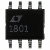
LT1801CS8#PBF Linear Technology, LT1801CS8#PBF Datasheet - Page 15

LT1801CS8#PBF
Manufacturer Part Number
LT1801CS8#PBF
Description
IC PREC OPAMP R-R DUAL LP 8-SOIC
Manufacturer
Linear Technology
Type
General Purpose Amplifierr
Datasheet
1.LT1801CS8PBF.pdf
(20 pages)
Specifications of LT1801CS8#PBF
Amplifier Type
General Purpose
Number Of Circuits
2
Output Type
Rail-to-Rail
Slew Rate
20 V/µs
Gain Bandwidth Product
70MHz
Current - Input Bias
400nA
Voltage - Input Offset
700µV
Current - Supply
1.8mA
Current - Output / Channel
50mA
Voltage - Supply, Single/dual (±)
2.3 V ~ 12.6 V, ±1.15 V ~ 6.3 V
Operating Temperature
0°C ~ 70°C
Mounting Type
Surface Mount
Package / Case
8-SOIC (3.9mm Width)
Rail/rail I/o Type
Rail to Rail Input/Output
Number Of Elements
2
Unity Gain Bandwidth Product
80MHz
Common Mode Rejection Ratio
85dB
Input Offset Voltage
3mV
Input Bias Current
1.5uA
Single Supply Voltage (typ)
3/5/9/12V
Dual Supply Voltage (typ)
±3/±5V
Voltage Gain In Db
98.59dB
Power Supply Rejection Ratio
78dB
Power Supply Requirement
Single/Dual
Shut Down Feature
No
Single Supply Voltage (min)
2.3V
Single Supply Voltage (max)
12.6V
Dual Supply Voltage (min)
±1.15V
Dual Supply Voltage (max)
±6.3V
Technology
BiCOM
Operating Temp Range
0C to 70C
Operating Temperature Classification
Commercial
Mounting
Surface Mount
Pin Count
8
Package Type
SOIC N
Lead Free Status / RoHS Status
Lead free / RoHS Compliant
-3db Bandwidth
-
Lead Free Status / Rohs Status
Compliant
Available stocks
Company
Part Number
Manufacturer
Quantity
Price
APPLICATIONS INFORMATION
output voltage is at half of either supply voltage (or the
maximum swing is less than 1/2 supply voltage). P
is given by:
Example: An LT1801 in an SO-8 package operating on ±5V
supplies and driving a 50Ω load, the worst-case power
dissipation is given by:
If both amplifi ers are loaded simultaneously, then the total
power dissipation is 0.34W.
The maximum ambient temperature that the part is
allowed to operate is:
Input Offset Voltage
The offset voltage will change depending upon which
input stage is active. The PNP input stage is active from
the negative supply rail to 1.2V from the positive supply
rail, then the NPN input stage is activated for the remain-
ing input range up to the positive supply rail during which
the PNP stage remains inactive. The offset voltage is
typically less than 75μV in the range that the PNP input
stage is active.
Input Bias Current
The LT1801/LT1802 employ a patent-pending technique
to trim the input bias current to less than 250nA for the
input common mode voltage of 0.2V above negative sup-
ply rail to 1.2V of the positive rail. The low input offset
voltage and low input bias current of the LT1801/LT1802
provide precision performance especially for high source
impedance applications.
P
P
T
A
DMAX
DMAX
= T
= 150°C – (0.34W • 190°C/W) = 85°C
J
= 0.17W
= (10 • 4.5mA) + (2.5)
– (P
= (V
DMAX
S
• I
SMAX
• 190°C/W)
) + (V
S
/2)
2
/50 = 0.045 + 0.125
2
/R
L
DMAX
Output
The LT1801/LT1802 can deliver a large output current,
so the short-circuit current limit is set around 50mA to
prevent damage to the device. Attention must be paid to
keep the junction temperature of the IC below the absolute
maximum rating of 150°C (refer to the Power Dissipation
section) when the output is continuously short circuited.
The output of the amplifi er has reverse-biased diodes
connected to each supply. If the output is forced beyond
either supply, unlimited current will fl ow through these
diodes. If the current is transient and limited to several
hundred mA and the total supply voltage is less than 12.6V,
the absolute maximum rating, no damage will occur to
the device.
Overdrive Protection
When the input voltage exceeds the power supplies, two
pairs of crossing diodes D1 to D4 will prevent the output
from reversing polarity. If the input voltage exceeds either
power supply by 700mV, diode D1/D2 or D3/D4 will turn
on to keep the output at the proper polarity. For the phase
reversal protection to perform properly, the input current
must be limited to less than 10mA. If the amplifi er is
severely overdriven, an external resistor should be used
to limit the overdrive current.
The LT1801/LT1802’s input stages are also protected
against a large differential input voltage of 1.4V or higher
by a pair of back-back diodes D5/D8 to prevent the emit-
ter-base breakdown of the input transistors. The current
in these diodes should be limited to less than 10mA when
they are active. The worst-case differential input voltage
usually occurs when the input is driven while the output
is shorted to ground in a unity gain confi guration. In ad-
dition, the amplifi er is protected against ESD strikes up
to 3kV on all pins by a pair of protection diodes on each
pin that are connected to the power supplies as shown
in Figure 1.
LT1801/LT1802
15
18012fc


