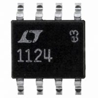
LT1124CS8#PBF Linear Technology, LT1124CS8#PBF Datasheet - Page 6

LT1124CS8#PBF
Manufacturer Part Number
LT1124CS8#PBF
Description
IC OP-AMP LOW NOISE DUAL 8-SOIC
Manufacturer
Linear Technology
Datasheet
1.LT1124CN8PBF.pdf
(18 pages)
Specifications of LT1124CS8#PBF
Amplifier Type
General Purpose
Number Of Circuits
2
Slew Rate
4.5 V/µs
Gain Bandwidth Product
12.5MHz
Current - Input Bias
8nA
Voltage - Input Offset
25µV
Current - Supply
2.3mA
Voltage - Supply, Single/dual (±)
±4 V ~ 18 V
Operating Temperature
0°C ~ 70°C
Mounting Type
Surface Mount
Package / Case
8-SOIC (3.9mm Width)
Lead Free Status / RoHS Status
Lead free / RoHS Compliant
Output Type
-
Current - Output / Channel
-
-3db Bandwidth
-
Available stocks
Company
Part Number
Manufacturer
Quantity
Price
ELECTRICAL CHARACTERISTICS
LT1124/LT1125
Note 1: Stresses beyond those listed under Absolute Maximum Ratings
may cause permanent damage to the device. Exposure to any Absolute
Maximum Rating condition for extended periods may affect device
reliability and lifetime.
Note 2: Typical parameters are defi ned as the 60% yield of parameter
distributions of individual amplifi ers; i.e., out of 100 LT1125s (or 100
LT1124s) typically 240 op amps (or 120) will be better than the indicated
specifi cation.
Note 3: This parameter is 100% tested for each individual amplifi er.
Note 4: This parameter is sample tested only.
Note 5: This parameter is not 100% tested.
Note 6: The inputs are protected by back-to-back diodes. Current limiting
resistors are not used in order to achieve low noise. If differential input
TYPICAL PERFORMANCE CHARACTERISTICS
6
0
0.1Hz to 10Hz Voltage Noise
2
TIME (SECONDS)
10.0
3.0
1.0
0.3
0.1
4
10
Current Noise vs Frequency
6
100
FREQUENCY (Hz)
8
1124/25 G01
1/f CORNER
100Hz
10
1k
MAXIMUM
TYPICAL
V
T
A
S
= ±15V
= 25°C
0.01Hz to 1Hz Voltage Noise
0
1124 G04
10k
20
TIME (SECONDS)
40
voltage exceeds ±1.4V, the input current should be limited to 25mA.
Note 7: Slew rate is measured in A
measured at ± 2.5V.
Note 8: 0.1Hz to 10Hz noise can be inferred from the 10Hz noise voltage
density test. See the test circuit and frequency response curve for 0.1Hz
to 10Hz tester in the Applications Information section of the LT1007 or
LT1028 data sheets.
Note 9: This parameter is guaranteed but not tested.
Note 10: The LT1124C/LT1125C and LT1124AC/LT1125AC are guaranteed
to meet specifi ed performance from 0°C to 70°C and are designed,
characterized and expected to meet these extended temperature limits,
but are not tested at –40°C and 85°C. The LT1124AI and LT1124I are
guaranteed to meet the extended temperature limits.
60
30
20
10
80
0
–75
1124/25 G02
Input Bias or Offset Current
vs Temperature
–50
100
–25
TEMPERATURE (°C)
0
100
30
10
3
1
0.1
25
LT1124AM/LT1125AM
Voltage Noise vs Frequency
V
LT1124M/LT1125M
= –1; input signal is ±7.5V, output
50
1.0
75
1/f CORNER
V
S
2.3Hz
FREQUENCY (Hz)
= ±15V
100
1124/25 G05
125
10
MAXIMUM
TYPICAL
100
V
T
S
A
= 25°C
= ±15V
1124/25 G03
11245fe
1000


