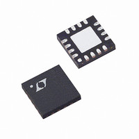
LTC6404IUD-2#PBF Linear Technology, LTC6404IUD-2#PBF Datasheet - Page 13

LTC6404IUD-2#PBF
Manufacturer Part Number
LTC6404IUD-2#PBF
Description
IC AMP/DRIVER DIFF 16-QFN
Manufacturer
Linear Technology
Type
ADC Driverr
Specifications of LTC6404IUD-2#PBF
Applications
Data Acquisition
Mounting Type
Surface Mount
Package / Case
16-WQFN Exposed Pad
Current - Supply
30.4mA
Operating Temperature
-40°C ~ 85°C
Output Type
Differential, Rail-to-Rail
Number Of Circuits
1
Current - Output / Channel
85mA
Amplifier Type
Differential
Voltage - Supply, Single/dual (±)
2.7 V ~ 5.5 V, ±1.35 V ~ 2.75 V
-3db Bandwidth
600MHz
Slew Rate
700 V/µs
Gain Bandwidth Product
900MHz
Current - Input Bias
23µA
Voltage - Input Offset
500µV
Number Of Channels
1
Number Of Elements
1
Power Supply Requirement
Single
Common Mode Rejection Ratio
60dB
Voltage Gain Db
90dB
Unity Gain Bandwidth Product (typ)
900MHz
Input Resistance
1@3V@-40C TO 85CMohm
Single Supply Voltage (typ)
3/5V
Dual Supply Voltage (typ)
Not RequiredV
Power Supply Rejection Ratio
60dB
Rail/rail I/o Type
Rail to Rail Output
Single Supply Voltage (min)
2.7V
Single Supply Voltage (max)
5.25V
Dual Supply Voltage (min)
Not RequiredV
Dual Supply Voltage (max)
Not RequiredV
Operating Temp Range
-40C to 85C
Operating Temperature Classification
Industrial
Mounting
Surface Mount
Pin Count
16
Package Type
QFN EP
No. Of Amplifiers
1
Input Offset Voltage
2mV
Gain Db Max
2dB
Bandwidth
900MHz
Supply Voltage Range
2.7V To 5.25V
Supply Current
30.4mA
Amplifier Case Style
QFN
Rohs Compliant
Yes
Lead Free Status / RoHS Status
Lead free / RoHS Compliant
Available stocks
Company
Part Number
Manufacturer
Quantity
Price
APPLICATIONS INFORMATION
When the feedback ratios mismatch (Δβ), common mode
to differential conversion occurs.
Setting the differential input to zero (V
gree of common mode to differential conversion is given
by the equation:
In general, the degree of feedback pair mismatch is a
source of common mode to differential conversion of
both signals and noise. Using 1% resistors or better will
mitigate most problems, and will provide about 41dB worst
case of common mode rejection. Using 0.1% resistors
will provide about 61dB of common mode rejection. A
low impedance ground plane should be used as a refer-
ence for both the input signal source, and the V
A direct short of V
V
ground plane, will further prevent common mode signals
from being converted to differential.
There may be concern on how feedback ratio mismatch
affects distortion. Distortion caused by feedback ratio mis-
match using 1% resistors or better is negligible. However,
in single supply level shifting applications where there is
a voltage difference between the input common mode
voltage and the output common mode voltage, resistor
mismatch can make the apparent voltage offset of the
amplifi er appear higher than specifi ed.
The apparent input referred offset induced by feedback
ratio mismatch is derived from the following equation:
Using the LTC6404-2 in a single supply application on a
single 5V supply with 1% resistors, and the input common
mode grounded, with the V
the worst case resistor mismatch can induce 22mV of
apparent offset voltage. With 0.1% resistors, the worst
case apparent offset reduces to 2.2mV.
OCM
V
V
OSDIFF(APPARENT)
OUTDIFF
(
V
with a high quality 0.1μF ceramic capacitor to this
INCM
= V
– V
OUT
OCM
OCM
+
)
•
≈ (V
– V
to this ground or bypassing the
OUT
AVG
ICM
OCM
–
V
– V
INDIFF
pin biased at mid-supply,
OCM
= 0
) • Δβ
INDIFF
= 0), the de-
OCM
pin.
Input Impedance and Loading Effects
The input impedance looking into the V
of Figure 1 depends on whether the sources V
V
(V
is simply:
For single ended inputs, because of the signal imbalance
at the input, the input impedance increases over the bal-
anced differential case. The input impedance looking into
either input is:
Input signal sources with non-zero output impedances can
also cause feedback imbalance between the pair of feedback
networks. For the best performance, it is recommended
that the source’s output impedance be compensated for.
If input impedance matching is required by the source,
R1 should be chosen (see Figure 4):
According to Figure 4, the input impedance looking into
the differential amp (R
case, thus:
R2 is chosen to balance R1 || R
INM
INP
R
R
R1=
R
R2 =
INP
INP
INM
= –V
are fully differential. For balanced input sources
= R
R
= R
R
R
=
R
INM
INM
I
I
INM
+ R
• R
INM
INM
1–
– R
• R
), the input impedance seen at either input
S
S
= R
2
=
1
S
S
•
I
1–
R
R
I
INM
I
2
R
1
+ R
F
•
) refl ects the single ended source
F
R
R
I
I
R
+ R
F
S
:
F
LTC6404-2
INP
or V
INM
INP
13
input
64042f
and


