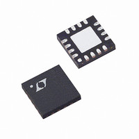
LTC6404IUD-2#PBF Linear Technology, LTC6404IUD-2#PBF Datasheet - Page 14

LTC6404IUD-2#PBF
Manufacturer Part Number
LTC6404IUD-2#PBF
Description
IC AMP/DRIVER DIFF 16-QFN
Manufacturer
Linear Technology
Type
ADC Driverr
Specifications of LTC6404IUD-2#PBF
Applications
Data Acquisition
Mounting Type
Surface Mount
Package / Case
16-WQFN Exposed Pad
Current - Supply
30.4mA
Operating Temperature
-40°C ~ 85°C
Output Type
Differential, Rail-to-Rail
Number Of Circuits
1
Current - Output / Channel
85mA
Amplifier Type
Differential
Voltage - Supply, Single/dual (±)
2.7 V ~ 5.5 V, ±1.35 V ~ 2.75 V
-3db Bandwidth
600MHz
Slew Rate
700 V/µs
Gain Bandwidth Product
900MHz
Current - Input Bias
23µA
Voltage - Input Offset
500µV
Number Of Channels
1
Number Of Elements
1
Power Supply Requirement
Single
Common Mode Rejection Ratio
60dB
Voltage Gain Db
90dB
Unity Gain Bandwidth Product (typ)
900MHz
Input Resistance
1@3V@-40C TO 85CMohm
Single Supply Voltage (typ)
3/5V
Dual Supply Voltage (typ)
Not RequiredV
Power Supply Rejection Ratio
60dB
Rail/rail I/o Type
Rail to Rail Output
Single Supply Voltage (min)
2.7V
Single Supply Voltage (max)
5.25V
Dual Supply Voltage (min)
Not RequiredV
Dual Supply Voltage (max)
Not RequiredV
Operating Temp Range
-40C to 85C
Operating Temperature Classification
Industrial
Mounting
Surface Mount
Pin Count
16
Package Type
QFN EP
No. Of Amplifiers
1
Input Offset Voltage
2mV
Gain Db Max
2dB
Bandwidth
900MHz
Supply Voltage Range
2.7V To 5.25V
Supply Current
30.4mA
Amplifier Case Style
QFN
Rohs Compliant
Yes
Lead Free Status / RoHS Status
Lead free / RoHS Compliant
Available stocks
Company
Part Number
Manufacturer
Quantity
Price
APPLICATIONS INFORMATION
LTC6404-2
Input Common Mode Voltage Range
The LTC6404-2’s input common mode voltage (V
defi ned as the average of the two input voltages, V
V
input common mode range depends on the circuit con-
fi guration (gain), V
fully differential input applications, where V
the common mode input voltage is approximately:
With singled ended inputs, there is an input signal com-
ponent to the input common mode voltage. Applying only
14
V
CM
V
Figure 4. Optimal Compensation for Signal Source Impedance
IN
V
INM
INP
V
V
–
+
–
+
–
. It extends from V
ICM
CM
V
V
VOCM
0.01μF
SHDN
0.1μF
•
=
V
V
+
–
Figure 5. Circuit for Common Mode Range
R1 CHOSEN SO THAT R1 || R
R2 CHOSEN TO BALANCE R1 || R
V
R
V
IN
S
F
R
+
+ R
1
2
3
4
F
SHDN
V
V
V
+ V
2
R2 = R
+
–
OCM
R
R
R
I
16
V
V
S
5
I
SHDN
I
+
–
IN
S
OCM
NC
NC
|| R1
–
V
V
R1
IN
IN
+
–
15
–
6
and V
to 1.4V below V
V
IN
IN
INM
+
V
–
+
–
OCM
R
OCM
R
F
F
R
= R
S
INM
S
CM
14
7
•
R
R
OUT
OUT
I
I
(Refer to Figure 5). For
R
–
+
V
V
I
OUTF
OUTF
13
8
R
+ R
–
+
–
+
I
OUTF
OUTF
R
R
LTC6404-2
V
F
F
+
F
–
+
+
V
V
+
–
–
–
64042 F05
. The operating
64042 F04
V
V
V
V
+
–
+
+
–
12
11
10
9
INP
V
V
OUT
OUT
0.1μF
0.1μF
= –V
–
+
IN
ICM
+
, and
INM
0.1μF
0.1μF
0.1μF
) is
V
V
V
+
–
–
,
V
approximately:
Output Common Mode Voltage Range
The output common mode voltage is defi ned as the aver-
age of the two outputs:
The V
mode feedback loop which internally forces V
The output common mode range extends from 1.1V above
V
voltage divider which sets the default mid-supply open
circuit potential.
In single supply applications, where the LTC6404-2 is
used to interface to an ADC, the optimal common mode
input range to the ADC is often determined by the ADC’s
reference. If the ADC makes a reference available for set-
ting the input common mode voltage, it can be directly
tied to the V
input impedance presented by the V
Electrical Characteristics Table. This impedance can be
assumed to be connected to a mid-supply potential. If an
external reference drives the V
bypassed with a high quality 0.01μF or larger capacitor to
a low impedance ground plane to fi lter any thermal noise
and to prevent common mode signals on this pin from
being inadvertently converted to differential signals.
Output Filter Considerations and Use
Filtering at the output of the LTC6404-2 is often desired
to provide either anti-aliasing or improved signal to noise
ratio. To simplify this fi ltering, the LTC6404-2 includes an
additional pair of differential outputs (OUTF
INP
–
V
V
V
to 1V below V
ICM
CM
OUTCM
(setting V
OCM
•
=
V
R
pin sets this average by an internal common
= V
IN
F
OCM
R
+
+ R
F
INM
OCM
+ V
2
pin, but must be capable of driving the
I
+
. The V
IN
to zero), the input common voltage is
=
+
–
V
V
OUT
INP
2
V
OCM
OCM
+
•
+ V
2
R
•
pin sits in the middle of a
OCM
OUT
F
R
R
+ R
F
I
–
pin, it should still be
R
+ R
I
OCM
I
F
as listed in the
OUT
+
+
and OUTF
+
= –V
OUT
64042f
–
–
)
.


