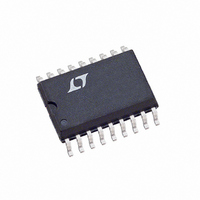
LTC1053CSW Linear Technology, LTC1053CSW Datasheet

LTC1053CSW
Specifications of LTC1053CSW
Available stocks
Related parts for LTC1053CSW
LTC1053CSW Summary of contents
Page 1
... Pin Compatible with Industry Standard Dual and Quad Op Amps U APPLICATIO S Thermocouple Amplifiers Electronic Scales Medical Instrumentation Strain Gauge Amplifiers High Resolution Data Acquisition DC Accurate R C Active Filters , LTC and LT are registered trademarks of Linear Technology Corporation. U TYPICAL APPLICATIO High Performance Low Cost Instrumentation Amplifier – ...
Page 2
... OUT D 13 – +IN D – LTC1053CN – OUT C N PACKAGE 14-LEAD PDIP = 65°C/W JA ORDER PART TOP VIEW NUMBER OUT D 16 –IN D LTC1053CSW 15 +IN D – + – OUT PACKAGE = 150°C, θ = 85°C/W JA LTC1051A TYP MAX MIN TYP ±0.5 ±5 ±0.5 ±0.0 ±0.05 ± ...
Page 3
ELECTRICAL CHARACTERISTICS temperature range, otherwise specifications are at T PARAMETER Input Noise Current Common Mode Rejection Ratio, CMRR Differential CMRR LTC1051, LTC1053 (Note 3) Power Supply Rejection Ratio Large Signal Voltage Gain Maximum Output Voltage Swing Slew Rate Gain Bandwidth ...
Page 4
LTC1051/LTC1053 W U TYPICAL PERFOR A CE CHARACTERISTICS Common Mode Input Range vs Supply Voltage – 2 – – 4 – 6 – ...
Page 5
W U TYPICAL PERFOR A CE CHARACTERISTICS Overload Recovery 400mV INPUT 0 0 OUTPUT – 5V 0.5ms A = –100 ±5V S LTC1051/LTC1053 DC to 10Hz Noise V = ± 25°C A 1µV TEST ...
Page 6
LTC1051/LTC1053 U U APPLICATIO S I FOR ATIO ACHIEVING PICOAMPERE/MICROVOLT PERFORMANCE Picoamperes In order to realize the picoampere level of accuracy of the LTC1051/LTC1053, proper care must be exercised. Leak- age currents in circuitry external to the amplifier can significantly ...
Page 7
U U APPLICATIO S I FOR ATIO =11V/V V 20mV/DIV =101V/V V 20mV/DIV 100µs/DIV (a) As the ambient temperature rises, the leakage current of the input protection devices increases, while ...
Page 8
LTC1051/LTC1053 U U APPLICATIO S I FOR ATIO LTC1051/LTC1053 as AC Amplifiers Although initially chopper stabilized op amps were de- signed to minimize DC offsets and offset drifts, the LTC1051/LTC1053 family, on top of its outstanding DC characteristics, presents efficient ...
Page 9
U U APPLICATIO S I FOR ATIO arbitrarily accept that “aliasing” occurs when output alias signals reach an amplitude of 0.01% or more of the output signal, then: the approximate minimum frequency input signal ...
Page 10
LTC1051/LTC1053 U U APPLICATIO S I FOR ATIO 5. For unity-gain inverting configuration, all the alias frequencies are 80dB to 84dB down from the output signal (Figures 6a, 6b). Combined with excellent THD under wide swing, the LTC1051/LTC1053 op amps ...
Page 11
U TYPICAL APPLICATIO S Obtaining Ultralow V Drift and Low Noise 1/2 – R4 LTC1051 1 – LTC1051 ...
Page 12
LTC1051/LTC1053 U TYPICAL APPLICATIO S Paralleling Choppers to Improve Noise NOTE: THIS CIRCUIT CAN ALSO BE USED DIFFERENCE AMPLIFIER FOR STRAIN GAUGES. CONNECT R2/3 AND R1/3 FROM NONINVERTING INPUTS, SHORTED TOGETHER, TO GROUND AND ...
Page 13
U TYPICAL APPLICATIO S Six Decade Log Amplifier 0.0022µ 0.1% 10k 0.1% 2 15.8k V – IN 1N4148 2M 0.1% 1 1/2 1nA < I <1mA IN LTC1051 LOG V –2V OUT ...
Page 14
LTC1051/LTC1053 PACKAGE DESCRIPTIO .300 BSC CORNER LEADS OPTION (7.62 BSC) .008 – .018 0° – 15° .045 – .068 (0.203 – 0.457) (1.143 – 1.650) FULL LEAD OPTION NOTE: LEAD DIMENSIONS APPLY TO SOLDER DIP/PLATE OR TIN PLATE LEADS .300 ...
Page 15
... Information furnished by Linear Technology Corporation is believed to be accurate and reliable. However, no responsibility is assumed for its use. Linear Technology Corporation makes no represen- tation that the interconnection of its circuits as described herein will not infringe on existing patent rights Package 16-Lead Plastic Small Outline (Wide 0 ...
Page 16
... V = ± ±8V 100dB S 120dB 0.1 1.0 5 30Hz IN RMS IN 1051/53 AC09 Dynamic Range 0.1 60dB V = ±5V S 80dB V = ±8V S 100dB 120dB 0.1 1.0 5 30Hz IN RMS IN 1051/53 AC11 (Max) = 16.5V SUPPLY LW/TP 1202 1K REV A • PRINTED IN USA LINEAR TECHNOLOGY CORPORATION 1990 10513fa ...


