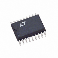
LTC1053CSW Linear Technology, LTC1053CSW Datasheet - Page 11

LTC1053CSW
Manufacturer Part Number
LTC1053CSW
Description
IC OPAMP CHOPR-STBL QUAD 18SOIC
Manufacturer
Linear Technology
Datasheet
1.LTC1051CN8PBF.pdf
(16 pages)
Specifications of LTC1053CSW
Amplifier Type
Chopper (Zero-Drift)
Number Of Circuits
4
Slew Rate
4 V/µs
Gain Bandwidth Product
2.5MHz
Current - Input Bias
15pA
Voltage - Input Offset
0.5µV
Current - Supply
1mA
Voltage - Supply, Single/dual (±)
4.75 V ~ 16 V, ±2.38 V ~ 8 V
Operating Temperature
0°C ~ 70°C
Mounting Type
Surface Mount
Package / Case
18-SOIC (7.5mm Width)
Lead Free Status / RoHS Status
Contains lead / RoHS non-compliant
Output Type
-
Current - Output / Channel
-
-3db Bandwidth
-
Other names
LTC1053CS
Available stocks
Company
Part Number
Manufacturer
Quantity
Price
Company:
Part Number:
LTC1053CSW
Manufacturer:
LT
Quantity:
5 510
Company:
Part Number:
LTC1053CSW
Manufacturer:
LINEAR
Quantity:
8
Part Number:
LTC1053CSW
Manufacturer:
LINEAR/凌特
Quantity:
20 000
Company:
Part Number:
LTC1053CSW#PBF
Manufacturer:
LT
Quantity:
368
Part Number:
LTC1053CSW#PBF
Manufacturer:
LINEAR/凌特
Quantity:
20 000
Part Number:
LTC1053CSW#TRPBF
Manufacturer:
LTNEAR
Quantity:
20 000
TYPICAL APPLICATIO S
** Noise measured in a 10 sec window. Peak-to-peak noise was also measured for 10 continuous minutes: With the LT1007 op amp the recorded noise was less than 0.2µV
+
–
* Interchange connections A and B .
LT1012*
and DC-10Hz.
LT1007
A1
B
A
2
3
3
2
–
+
+
–
Obtaining Ultralow V
LTC1051
1
1/2
R1
A1
750Ω
5V
R1
3k
8
R2
1
6
OUT
R3
R4
V
57Ω
S
R2
2k
= ±5V
5
6
+
–
OS
LTC1051
R5
1/2
Drift and Low Noise
C2
340k
250k
R3
C1
U
7
10k
10k
R4
LTC1051/LT1007 Peak-to-Peak Noise
100k
100k
R5
1051/53 AC01a
OUT
0.01µF
0.01µF
1 SEC/DIV
C1
The dual chopper op amp buffers the inputs of A1 and
corrects its offset voltage and offset voltage drift. With the
R, C values shown, the power-up warm up time is typically
20 seconds. The step response of the composite amplifier
does not present settling tails. The LT1007 should be used
when extremely low noise; V
when the input source resistance is low—for instance a
350Ω strain gauge bridge. The LT1012 or equivalent
should be used when low bias current (100pA) is also
required in conjunction with DC to 10Hz low noise and low
V
voltages were less than 2µV.
OS
and V
DC TO 1Hz
0.001µF
0.001µF
NOISE
C2
OS
drift. The measured typical input offset
e
DC TO 10Hz
OUT
LTC1051/LTC1053
NOISE
(DC – 1Hz)**
0.1µV
0.3µV
P-P
P-P
OS
and V
1051/53 AC01b
OS
e
OUT
drift are sought
(DC – 10Hz)**
0.15µV
0.4µV
P-P
for both DC-1Hz
P-P
P-P
11
10513fa


