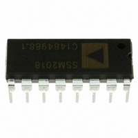
SSM2018PZ Analog Devices Inc, SSM2018PZ Datasheet - Page 10

SSM2018PZ
Manufacturer Part Number
SSM2018PZ
Description
IC AMP AUDIO MONO CLASS AB 16DIP
Manufacturer
Analog Devices Inc
Datasheet
1.SSM2018PZ.pdf
(16 pages)
Specifications of SSM2018PZ
Amplifier Type
Audio
Number Of Circuits
1
Slew Rate
5 V/µs
Gain Bandwidth Product
14MHz
Current - Input Bias
250nA
Voltage - Input Offset
1000µV
Current - Supply
11mA
Voltage - Supply, Single/dual (±)
10 V ~ 36 V, ±5 V ~ 18 V
Operating Temperature
-40°C ~ 85°C
Mounting Type
Through Hole
Package / Case
16-DIP (0.300", 7.62mm)
Amplifier Class
AB
No. Of Channels
1
Supply Voltage Range
± 5V To ± 18V
Load Impedance
100kohm
Operating Temperature Range
-40°C To +85°C
Amplifier Case Style
DIP
No. Of Pins
16
Rohs Compliant
Yes
Lead Free Status / RoHS Status
Lead free / RoHS Compliant
Output Type
-
Current - Output / Channel
-
-3db Bandwidth
-
Lead Free Status / Rohs Status
RoHS Compliant part
Electrostatic Device
Available stocks
Company
Part Number
Manufacturer
Quantity
Price
Company:
Part Number:
SSM2018PZ
Manufacturer:
MICROCHIP
Quantity:
1 001
SSM2018T
Proper Operating Mode for the SSM2018T
The SSM2018T has the flexibility of operating in either Class A
or Class AB. This is accomplished by adjusting the amount of
current flowing in the gain core (I
trade-off between the two classes is that Class A tends to have
lower THD but higher noise than Class AB. However, by using
well matched gain core transistors, distortion compensation
circuitry and laser trimming, the SSM2018T has excellent THD
performance in Class AB. Thus, it offers the best of both worlds
in having the low noise of Class AB with low THD.
Because the SSM2018T operates optimally in Class AB, the
distortion trim is performed for this class. To guarantee conform-
ance to the data sheet THD specifications, the SSM2018T must be
operated in class AB. This does not mean that it can not be oper-
ated in Class A, but the optimal THD trim point is different for
the two classes. Using Class A operation results to 0.05% with-
out trim. An external potentiometer could be added to change
the trim back to its optimal point as shown in the OVCE appli-
cation circuit, but this adds the expense and time in adjusting a
potentiometer.
The class of operation is set by selecting the proper value for R
shown in Figure 1. R
MODE input (Pin 12). For class AB operation with ± 15 V
supplies, R
95 mA. For other supply voltages, adjust the value of R
that current remains at 95 mA. This current follows the formula:
The factor of 0.7 V arises from the fact that the dc bias on Pin
12 is a diode drop above ground.
Output Drive
The SSM2018T is buffered by an internal op amp to provide a low
impedance output. This output is capable of driving to within
1.2 V of either rail at 1% distortion for a 100 kW load. Note: This
100 kW load is in parallel with the feedback resistor of 18 kW, so
the effective load is 15.3 kW. For better than 0.01% distortion,
the output should remain about 3.5 V away from either rail as
shown in TPC 2. As the graph of output swing versus load resis-
tance shows (TPC 9), to maintain less than 1% distortion the
output current should be limited to approximately ±1.3 mA. If
higher current drive is required, the output should be buffered with
a high quality op amp such as the OP176 or AD797.
The internal amplifiers are compensated for unity gain stability
and are capable of driving a capacitive load up to 4700 pF.
Larger capacitive loads should be isolated from the output of the
SSM2018T by the use of a 50 W series resistor.
I
MODE
=
B
(V
should be 150 kW. This results in a current of
CC
R
– 0.7V )
B
B
determines the current flowing into the
M
in Figure 2). The traditional
B
such
(3)
B
–10–
Upgrading SSM2018 Sockets
The SSM2018T easily replaces the SSM2018 in the basic VCA
configuration. The parts are pin for pin compatible allowing
direct replacement. At the same time, the trimming potentiom-
eters for symmetry and offset should be removed, as shown in
Figure 3. Upgrading immediately to the SSM2018T saves the
expense of the potentiometers and the time in production of
trimming for minimum distortion and control feedthrough.
If the SSM2018 is used in the OVCE or VCP configuration, the
SSM2018T can still directly replace it; however, the potentiom-
eters cannot necessarily be removed, as explained in the OVCE
and VCP sections.
Temperature Compensation of the Gain Constant
As explained above, the gain constant has a –3500 ppm/∞C
temperature drift due to the inherent nature of the control port.
Over the full temperature range of –40∞C to +85∞C, the drift
causes the gain to change by 7 dB if the part is in a gain of
± 20 dB. If the application requires the gain constant to be the
same over a wide temperature range, external temperature com-
pensation should be employed. The simplest form of compensa-
tion is a temperature compensating resistor (TCR) such as the
PT146 from Precision Resistor Co. These elements are different
than a standard thermistor in that they are linear over tempera-
ture to better match the linear drift of the gain constant.
Figure 4. Two TCRs Compensate for Temperature Drift of
Gain Constant
V
V
IN+
IN–
V+
V–
CONTROL
VOLTAGE
OFFSET
TRIM
100k
1 F 18k
1 F
R
NC = NO CONNECT
B
: 150k
Figure 3. Upgrading SSM2018 Sockets
18k
V+
10M
REMOVE FOR SSM2018T
FOR CLASS AB
2k
47pF
SYMMETRY
TRIM
500k
SSM2018T
OP27
470k
1k *
18k
50pF
+15V
–15V
NC
*PT146 AVAILABLE FROM
PIN 11
SSM2018T
PRECISION RESISTOR CO.
10601 75
LARGO, FL 34647
(813) 541-5771
V–
R
1 F
B
V
TH
OUT
ST. NORTH
V+
1k
3k
V
CONTROL
REV. B


