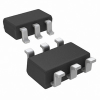
LMH6639MF/NOPB National Semiconductor, LMH6639MF/NOPB Datasheet - Page 16

LMH6639MF/NOPB
Manufacturer Part Number
LMH6639MF/NOPB
Description
IC AMP 190MHZ R-R OTPT SOT23-6
Manufacturer
National Semiconductor
Series
VIP10™r
Datasheet
1.LMH6639MFNOPB.pdf
(20 pages)
Specifications of LMH6639MF/NOPB
Amplifier Type
Voltage Feedback
Number Of Circuits
1
Output Type
Rail-to-Rail
Slew Rate
200 V/µs
Gain Bandwidth Product
90MHz
-3db Bandwidth
228MHz
Current - Input Bias
1.4µA
Voltage - Input Offset
1030µV
Current - Supply
4.18mA
Current - Output / Channel
112mA
Voltage - Supply, Single/dual (±)
3 V ~ 12 V, ±1.5 V ~ 6 V
Operating Temperature
-40°C ~ 85°C
Mounting Type
Surface Mount
Package / Case
SOT-23-6
Number Of Channels
1
Voltage Gain Db
100 dB
Common Mode Rejection Ratio (min)
72 dB
Input Voltage Range (max)
12 V
Input Voltage Range (min)
3 V
Input Offset Voltage
5 mV
Operating Supply Voltage
5 V, 9 V
Supply Current
3.6 mA
Maximum Operating Temperature
+ 85 C
Mounting Style
SMD/SMT
Maximum Dual Supply Voltage
+/- 6 V
Minimum Operating Temperature
- 40 C
Lead Free Status / RoHS Status
Lead free / RoHS Compliant
Other names
LMH6639MF
LMH6639MFTR
LMH6639MFTR
Available stocks
Company
Part Number
Manufacturer
Quantity
Price
www.national.com
Note: Pin numbers pertain to SOIC-8 package
Multiplexing signals “FREQ 1” and “FREQ 2” exhibit closed
loop non-inverting gain of +2 each based upon identical
330Ω resistors in the gain setting positions of IC1 and IC2.
The two multiplexing signals are combined at the input of IC3,
which is the third LMH6639. This amplifier may be used as a
unity gain buffer or may be used to set a particular gain for
the circuit.
1k resistors are used to set an inverting gain of −1 for IC3 in
the circuit of
duced. The upper trace shows the switching waveform used
to switch between the 5MHz and 10MHz multiplex signals.
FIGURE 5. Switching between 5 and 10MHz
Figure
4.
Figure 5
illustrates the waveforms pro-
20030248
FIGURE 4. Multiplexer
16
The lower trace shows the output waveform consisting of
5MHz and 10MHz signals corresponding to the high or low
state of the switching signal.
In the circuit of
together such that their output impedances are placed in par-
allel at the input of IC3. The output impedance of the disabled
amplifier is high compared both to the output impedance of
the active amplifier and the 330Ω gain setting resistors. The
closed loop output resistance for the LMH6639 is around
0.2Ω. Thus the active state amplifier output impedance dom-
inates the input node to IC3, while the disabled amplifier is
assured of a high level of suppression of unwanted signals
which might be present at the output.
SHUTDOWN OPERATION
With SD pin left floating, the device enters normal operation.
However, since the SD pin has high input impedance, it is best
tied to V
shutdown due to capacitive pick-up from nearby nodes.
LMH6639 will typically go into shutdown when SD pin is more
than 1.7V below V
The SD pin can be driven by push-pull or open collector (open
drain) output logic. Because the LMH6639's shutdown is ref-
erenced to V+, interfacing to the shutdown logic is rather
simple, for both single and dual supply operation, with either
form of logic used. Typical configurations are shown in
6
and
Figure 7
+
for normal operation. This will avoid inadvertent
below for push-pull output:
Figure
+
, regardless of operating supplies.
4, the outputs of IC1 and IC2 are tied
20030247
Figure


