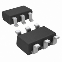
LMH6639MF/NOPB National Semiconductor, LMH6639MF/NOPB Datasheet - Page 17

LMH6639MF/NOPB
Manufacturer Part Number
LMH6639MF/NOPB
Description
IC AMP 190MHZ R-R OTPT SOT23-6
Manufacturer
National Semiconductor
Series
VIP10™r
Datasheet
1.LMH6639MFNOPB.pdf
(20 pages)
Specifications of LMH6639MF/NOPB
Amplifier Type
Voltage Feedback
Number Of Circuits
1
Output Type
Rail-to-Rail
Slew Rate
200 V/µs
Gain Bandwidth Product
90MHz
-3db Bandwidth
228MHz
Current - Input Bias
1.4µA
Voltage - Input Offset
1030µV
Current - Supply
4.18mA
Current - Output / Channel
112mA
Voltage - Supply, Single/dual (±)
3 V ~ 12 V, ±1.5 V ~ 6 V
Operating Temperature
-40°C ~ 85°C
Mounting Type
Surface Mount
Package / Case
SOT-23-6
Number Of Channels
1
Voltage Gain Db
100 dB
Common Mode Rejection Ratio (min)
72 dB
Input Voltage Range (max)
12 V
Input Voltage Range (min)
3 V
Input Offset Voltage
5 mV
Operating Supply Voltage
5 V, 9 V
Supply Current
3.6 mA
Maximum Operating Temperature
+ 85 C
Mounting Style
SMD/SMT
Maximum Dual Supply Voltage
+/- 6 V
Minimum Operating Temperature
- 40 C
Lead Free Status / RoHS Status
Lead free / RoHS Compliant
Other names
LMH6639MF
LMH6639MFTR
LMH6639MFTR
Available stocks
Company
Part Number
Manufacturer
Quantity
Price
Common voltages for logic gates are +5V or +3V. To ensure
proper power on/off with these supplies, the logic should be
able to swing to 3.4V and 1.4V minimum, respectively.
LMH6639’s shutdown pin can also be easily controlled in ap-
plications where the analog and digital sections are operated
at different supplies.
logic output, SD, can turn the LMH6639 on and off, indepen-
dent of what supplies are used for the analog and the digital
sections:
FIGURE 8. Shutdown Interface (Single Supply, Open
FIGURE 6. Shutdown Interface (Single Supply)
FIGURE 7. Shutdown Interface (Dual Supplies)
Figure 8
Collector Logic)
shows a configuration where a
20030272
20030271
20030273
17
The LMH6639 has an internal pull-up resistor on SD such that
if left un-connected, the device will be in normal operation.
Therefore, no pull-up resistor is needed on this pin. Another
common application is where the transistor in
would be internal to an open collector (open drain) logic gate;
the basic connections will remain the same as shown.
PCB LAYOUT CONSIDERATION AND COMPONENTS
SELECTION
Care should be taken while placing components on a PCB.
All standard rules should be followed especially the ones for
high frequency and/ or high gain designs. Input and output
pins should be separated to reduce cross-talk, especially un-
der high gain conditions. A groundplane will be helpful to
avoid oscillations. In addition, a ground plane can be used to
create micro-strip transmission lines for matching purposes.
Power supply, as well as shutdown pin de-coupling will re-
duce cross-talk and chances of oscillations.
Another important parameter in working with high speed am-
plifiers is the component values selection. Choosing high
value resistances reduces the cut-off frequency because of
the influence of parasitic capacitances. On the other hand
choosing the resistor values too low could "load down" the
nodes and will contribute to higher overall power dissipation.
Keeping resistor values at several hundreds of ohms up to
several kΩ will offer good performance.
National Semiconductor suggests the following evaluation
boards as a guide for high frequency layout and as an aid in
device testing and characterization:
These free evaluation boards are shipped when a device
sample request is placed with National Semiconductor. For
normal operation, tie the SD pin to V
LMH6639MA
LMH6639MF
Device
8-Pin SOIC
Package
SOT23-6
+
.
Evaluation Board
CLC730027
CLC730116
Figure 8
PN
www.national.com
above,


