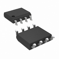
LMH6703MA/NOPB National Semiconductor, LMH6703MA/NOPB Datasheet - Page 11

LMH6703MA/NOPB
Manufacturer Part Number
LMH6703MA/NOPB
Description
IC OPAMP 1.2GHZ SHUTDOWN 8SOIC
Manufacturer
National Semiconductor
Series
PowerWise®r
Datasheet
1.LMH6703MFNOPB.pdf
(13 pages)
Specifications of LMH6703MA/NOPB
Amplifier Type
Current Feedback
Number Of Circuits
1
Slew Rate
4500 V/µs
-3db Bandwidth
1.8GHz
Current - Input Bias
7µA
Voltage - Input Offset
1500µV
Current - Supply
11mA
Current - Output / Channel
90mA
Voltage - Supply, Single/dual (±)
8 V ~ 12 V, ±4 V ~ 6 V
Operating Temperature
-40°C ~ 85°C
Mounting Type
Surface Mount
Package / Case
8-SOIC (3.9mm Width)
Number Of Channels
1
Common Mode Rejection Ratio (min)
45 dB
Input Offset Voltage
7 mV at +/- 5 V
Supply Current
12.5 mA at +/- 5 V
Maximum Operating Temperature
+ 85 C
Maximum Dual Supply Voltage
+/- 6 V
Minimum Operating Temperature
- 40 C
For Use With
LMH730227 - BOARD EVALUATION FOR SOIC PKGLMH730165 - BOARD EVALUATIONLMH730216 - BOARD EVAL HS MONO AMP SOT23
Lead Free Status / RoHS Status
Lead free / RoHS Compliant
Output Type
-
Gain Bandwidth Product
-
Lead Free Status / Rohs Status
Details
Other names
*LMH6703MA
*LMH6703MA/NOPB
LMH6703MA
*LMH6703MA/NOPB
LMH6703MA
Application Section
VIDEO PERFORMANCE
The LMH6703 has been designed to provide excellent per-
formance with production quality video signals in a wide
variety of formats such as HDTV and High Resolution VGA.
NTSC and PAL performance is nearly flawless with DG of
0.01% and DP of 0.02˚. Best performance will be obtained
with back terminated loads. The back termination reduces
reflections from the transmission line and effectively masks
transmission line and other parasitic capacitance from the
amplifier output stage. Figure 5 shows a typical configuration
for driving 75Ω cable. The amplifier is configured for a gain of
two compensating for the 6 dB loss due to R
ENABLE/DISABLE
FIGURE 6. SD Pin Simplified Schematic
FIGURE 5. Typical Video Application
(SOT23 Pinout Shown)
(Continued)
OUT
.
20110633
20110637
11
For
patible disable function. Apply a logic low (
pin and the LMH6703 is disabled. Apply a logic high (
or let the pin float and the LMH6703 is enabled. Voltage, not
current, at the Shutdown pin (SD) determines the enable/
disable state. Care must be exercised to prevent the shut-
down pin voltage from going more than 0.8V below the
midpoint of the supply voltages (0V with split supplies, V
with single supply biasing). Doing so could cause transistor
Q1 to Zener resulting in damage to the disable circuit (See
Figure 6). The core amplifier is unaffected by this, but the
shutdown operation could become permanently slower as a
result.
Disabled, the LMH6703 inputs and output become high im-
pedances. While disabled the LMH6703 quiescent current is
approximately 200 µA. Because of the pull up resistor on the
shutdown circuit, the I
negative supply currents respectively) are not balanced in
the disabled state. The positive supply current (I
proximately 300 µA while the negative supply current (I
only 200 µA. The remaining I
through the shutdown pin.
The disable function can be used to create analog switches
or multiplexers. Implement a single analog switch with one
LMH6703 positioned between an input and output. Create
an analog multiplexer with several LMH6703’s and tie the
outputs together.
±
5V supplies only the LMH6703 has a TTL logic com-
CC
and I
EE
EE
current of 100 µA flows
currents (positive and
<
.8V) to the SD
www.national.com
CC
>
) is ap-
2.0V),
EE
) is
+
/2


