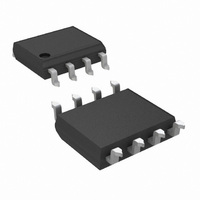
LMH6703MA/NOPB National Semiconductor, LMH6703MA/NOPB Datasheet - Page 9

LMH6703MA/NOPB
Manufacturer Part Number
LMH6703MA/NOPB
Description
IC OPAMP 1.2GHZ SHUTDOWN 8SOIC
Manufacturer
National Semiconductor
Series
PowerWise®r
Datasheet
1.LMH6703MFNOPB.pdf
(13 pages)
Specifications of LMH6703MA/NOPB
Amplifier Type
Current Feedback
Number Of Circuits
1
Slew Rate
4500 V/µs
-3db Bandwidth
1.8GHz
Current - Input Bias
7µA
Voltage - Input Offset
1500µV
Current - Supply
11mA
Current - Output / Channel
90mA
Voltage - Supply, Single/dual (±)
8 V ~ 12 V, ±4 V ~ 6 V
Operating Temperature
-40°C ~ 85°C
Mounting Type
Surface Mount
Package / Case
8-SOIC (3.9mm Width)
Number Of Channels
1
Common Mode Rejection Ratio (min)
45 dB
Input Offset Voltage
7 mV at +/- 5 V
Supply Current
12.5 mA at +/- 5 V
Maximum Operating Temperature
+ 85 C
Maximum Dual Supply Voltage
+/- 6 V
Minimum Operating Temperature
- 40 C
For Use With
LMH730227 - BOARD EVALUATION FOR SOIC PKGLMH730165 - BOARD EVALUATIONLMH730216 - BOARD EVAL HS MONO AMP SOT23
Lead Free Status / RoHS Status
Lead free / RoHS Compliant
Output Type
-
Gain Bandwidth Product
-
Lead Free Status / Rohs Status
Details
Other names
*LMH6703MA
*LMH6703MA/NOPB
LMH6703MA
*LMH6703MA/NOPB
LMH6703MA
Application Section
GENERAL DESCRIPTION
The LMH6703 is a high speed current feedback amplifier,
optimized for excellent bandwidth, gain flatness, and low
distortion. The loop gain for a current feedback op amp, and
hence the frequency response, is predominantly set by the
feedback resistor value. The LMH6703 in the SOT23-6 pack-
age is optimized for use with a 560Ω feedback resistor. The
LMH6703 in the SOIC package is optimized for use with a
390Ω feedback resistor. Using lower values can lead to
excessive ringing in the pulse response while a higher value
will limit the bandwidth. Application Note OA-13 discusses
this in detail along with the occasions where a different R
might be advantageous.
EVALUATION BOARDS
Device
LMH6703MF
LMH6703MA
FIGURE 1. Recommended Non-Inverting Gain Circuit
FIGURE 2. Recommended Inverting Gain Circuit
(SOIC Pinout Shown)
(SOIC Pinout Shown)
Package
SOT23-6
SOIC
Evaluation Board
Part Number
CLC730216
CLC730227
20110604
20110603
F
9
An Evaluation Board is shipped upon request when a
sample order is placed with National Semiconductor.
FEEDBACK RESISTOR SELECTION
One of the key benefits of a current feedback operational
amplifier is the ability to maintain optimum frequency re-
sponse independent of gain by using appropriate values for
the feedback resistor (R
Typical Performance plots specify an R
the SOIC package), a gain of +2 V/V and
plies (unless otherwise specified). Generally, lowering R
from it’s recommended value will peak the frequency re-
sponse and extend the bandwidth while increasing the value
of R
Reducing the value of R
value will cause overshoot, ringing and, eventually, oscilla-
tion.
Since a current feedback amplifier is dependant on the value
of R
value of R
different packages use different R
Figure 3, Recommended R
SOIC package use different values for the feedback resistor,
R
some experimentation to find the optimal R
circuit. In general, a value of R
peaking is the best compromise between stability and maxi-
mum bandwidth. Note that it is not possible to use a current
feedback amplifier with the output shorted directly to the
inverting input. The buffer configuration of the LMH6703
requires a 560Ω (390Ω for SOIC package) feedback resistor
for stable operation.
The LMH6703 was optimized for high speed operation. As
shown in Figure 3, the suggested value for R
higher gains. Due to the output impedance of the input
buffer, there is a practical limit for how small R
based on the lowest practical value of R
applies to both inverting and non inverting configurations.
For the LMH6703 the input resistance of the inverting input is
approximately 30Ω and 20Ω is a practical (but not hard and
fast) lower limit for R
gain bandwidth limited fashion in the region when R
nearly equal to the input buffer impedance. Note that the
F
. Since each application is slightly different, it is worth
F
F
will cause the frequency response to roll off faster.
to provide frequency compensation and since the
FIGURE 3. Recommended R
F
can be used to optimize the frequency response,
G
. The LMH6703 begins to operate in a
F
). The Electrical Characteristics and
F
F
too far below it’s recommended
vs. Gain, the SOT23-6 and the
F
that produces ≈0.1 dB of
F
values. As shown in
F
F
of 560Ω (390Ω for
vs. Gain
G
±
. This limitation
F
5V power sup-
F
decreases for
20110639
for a given
www.national.com
F
can go,
G
is
F


