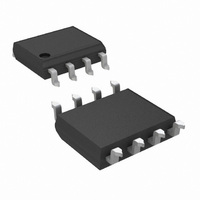
LMP2022MA/NOPB National Semiconductor, LMP2022MA/NOPB Datasheet - Page 14

LMP2022MA/NOPB
Manufacturer Part Number
LMP2022MA/NOPB
Description
IC OP AMP DUAL LOW NOISE 8SOIC
Manufacturer
National Semiconductor
Series
LMP®r
Datasheet
1.LMP2021MAEVAL.pdf
(20 pages)
Specifications of LMP2022MA/NOPB
Amplifier Type
Chopper (Zero-Drift)
Number Of Circuits
2
Slew Rate
2.6 V/µs
Gain Bandwidth Product
5MHz
Current - Input Bias
25pA
Voltage - Input Offset
0.4µV
Current - Supply
1.1mA
Current - Output / Channel
50mA
Voltage - Supply, Single/dual (±)
2.2 V ~ 5.5 V
Operating Temperature
-40°C ~ 125°C
Mounting Type
Surface Mount
Package / Case
8-SOIC (3.9mm Width)
Lead Free Status / RoHS Status
Lead free / RoHS Compliant
Output Type
-
-3db Bandwidth
-
Other names
*LMP2022MA/NOPB
LMP2022MA
LMP2022MA
www.national.com
* No significant difference in Noise measurements at
A
INPUT BIAS CURRENT
The bias current of the LMP2021/LMP2022 behaves differ-
ently than a conventional amplifier due to the dynamic tran-
LOWERING THE INPUT BIAS CURRENT
As mentioned in the INPUT BIAS CURRENT section, the in-
put bias current of an auto zero amplifier such as the
LMP2021/LMP2022 varies with input impedance and feed-
back impedance. Once the value of a certain input resistance,
i.e. sensor resistance, is known, it is possible to optimize the
input bias current for this fixed input resistance by choosing
the capacitance value that minimizes that current. Figure 7
shows the input bias current vs. input impedance of the
LMP2021/LMP2022. The value of R
this test is 1 GΩ. When this value of input resistance is used,
and when a parallel capacitance of 22 pF is placed on the
circuit, the resulting input bias current is nearly 0 pA.
Figure 7 can be used to extrapolate capacitor values for other
sensor resistances. For this purpose, the total impedance
seen by the input of the LMP2021/LMP2022 needs to be cal-
culated based on Figure 7. By knowing the value of R
can calculate the corresponding C
inverting input bias current, positive bias current, value.
Amplifier
V
(V/V)
1000
Gain
100
= 10V/V
10
Table 1: RMS Input Noise Performance
Requirement
Bandwidth
System
1000
1000
1000
(Hz)
100
100
100
10
FIGURE 6. Input Bias Current of LMP2021/LMP2022 is lower than Competitor A
LMP2021/LMP2022
Figure 3
Circuit
229
763
229
763
158
608
71
RMS Input Noise (nV)
G
which minimizes the non-
G
Figure 4
Circuit
or input resistance in
196
621
146
462
46
*
*
Figures 4, 3
Competitor
Circuit
1030
1030
1030
300
300
300
95
A
G
, one
14
sient currents created on the input of an auto-zero circuit. The
input bias current is affected by the charge and discharge
current of the input auto-zero circuit. The amount of current
sunk or sourced from that stage is dependent on the combi-
nation of input impedance (resistance and capacitance), as
well as the balance and matching of these impedances across
the two inputs. This current, integrated in the auto-zero circuit,
causes a shift in the apparent "bias current". Because of this,
there is an apparent "bias current vs. input impedance" inter-
action. In the LMP2021/LMP2022 for an input resistive
impedance of 1 GΩ, the shift in input bias current can be up
to 40 pA. This input bias shift is caused by varying the input's
capacitive impedance. Since the input bias current is depen-
dent on the input impedance, it is difficult to estimate what the
actual bias current is without knowing the end circuit and as-
sociated capacitive strays.
Figure 6 shows the input bias current of the LMP2021/
LMP2022 and that of another commercially available ampli-
fier from a competitor. As it can be seen, the shift in LMP2021/
LMP2022 bias current is much lower than that of other chop-
per style or auto zero amplifiers available from other vendors.
FIGURE 7. Input Bias Current vs. C
30014975
G
with R
30014964
G
= 1 GΩ


