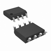
LMP2022MA/NOPB National Semiconductor, LMP2022MA/NOPB Datasheet - Page 15

LMP2022MA/NOPB
Manufacturer Part Number
LMP2022MA/NOPB
Description
IC OP AMP DUAL LOW NOISE 8SOIC
Manufacturer
National Semiconductor
Series
LMP®r
Datasheet
1.LMP2021MAEVAL.pdf
(20 pages)
Specifications of LMP2022MA/NOPB
Amplifier Type
Chopper (Zero-Drift)
Number Of Circuits
2
Slew Rate
2.6 V/µs
Gain Bandwidth Product
5MHz
Current - Input Bias
25pA
Voltage - Input Offset
0.4µV
Current - Supply
1.1mA
Current - Output / Channel
50mA
Voltage - Supply, Single/dual (±)
2.2 V ~ 5.5 V
Operating Temperature
-40°C ~ 125°C
Mounting Type
Surface Mount
Package / Case
8-SOIC (3.9mm Width)
Lead Free Status / RoHS Status
Lead free / RoHS Compliant
Output Type
-
-3db Bandwidth
-
Other names
*LMP2022MA/NOPB
LMP2022MA
LMP2022MA
In a typical I-V converter, the output voltage will be the sum
of DC offset plus bias current and the applied signal through
the feedback resistor. In a conventional input stage, the in-
verting input's capacitance has very little effect on the circuit.
This effect is generally on settling time and the dielectric
soakage time and can be ignored. In auto zero amplifiers, the
input capacitance effect will add another term to the output.
This additional term means that the baseline reading on the
output will be dependent on the input capacitance. The term
input capacitance for this purpose includes circuit strays and
any input cable capacitances. There is a slight variation in the
capacitive offset as the duty cycle and amplitude of the pulses
vary from part to part, depending on the correction at the time.
The lowest input current will be obtained when the
impedances, both resistive and capacitive, are matched be-
tween the inputs. By balancing the input capacitances, the
effect can be minimized. A simple way to balance the input
impedance is adding a capacitance in parallel to the feedback
resistance. The addition of this feedback capacitance re-
duces the bias current and increases the stability of the
operational amplifier. Figure 8 shows the input bias current of
the LMP2021/LMP2022 when R
seen from Figure 8, choosing the optimum value of C
help reducing the input bias current.
The effect of bias current on a circuit can be estimated with
the following:
Where A
I
tively. It is common to show the average of these bias currents
in product datasheets. If I
specified, use the I
tables for this calculation.
For the application circuit shown in Figure 12, the LMP2022
amplifiers each have a gain of 18. With a sensor impedance
of 500Ω for the bridge, and using the above equation, the total
error due to the bias current on the outputs of the LMP2022
amplifier will be less than 200 nV.
BIAS−
FIGURE 8. Input Bias Current vs. C
denote the positive and negative bias current, respec-
V
is the closed loop gain of the system and I
BIAS
A
V
*I
BIAS+
value provided in datasheet graphs or
BIAS+
*Z
S
and I
- I
F
is set to 1 GΩ. As it can be
BIAS−
BIAS−
*Z
F
F
are not individually
with R
30014965
F
= 1 GΩ
BIAS+
F
and
will
15
SENSOR IMPEDANCE
The sensor resistance, or the resistance connected to the in-
puts of the LMP2021/LMP2022, contributes to the total
impedance seen by the auto correcting input stage.
As shown in Figure 9, the sum of R
a low pass filter with C
increases, the time constant of this filter increases, resulting
in a slower output signal which could have the effect of re-
ducing the open loop gain, A
In order to prevent this reduction in A
impedance sensors or other high resistances connected to
the input of the LMP2021/LMP2022, a capacitor can be
placed in parallel to this input resistance. This is shown in
Figure 10
FIGURE 10. Sensor Impedance with Parallel Capacitance
FIGURE 9. Auto Correcting Input Stage Model
OUT
during correction cycles. As R
VOL
, of the LMP2021/LMP2022.
IN
and R
VOL
in presence of high
ON-SWITCH
www.national.com
30014969
30014967
will form
30014968
30014970
IN


