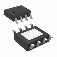
LM7372MR/NOPB National Semiconductor, LM7372MR/NOPB Datasheet - Page 10

LM7372MR/NOPB
Manufacturer Part Number
LM7372MR/NOPB
Description
IC OPAMP DUAL HS HI OUTP 8-PSOP
Manufacturer
National Semiconductor
Series
VIP™ IIIr
Datasheet
1.LM7372IMANOPB.pdf
(16 pages)
Specifications of LM7372MR/NOPB
Amplifier Type
Voltage Feedback
Number Of Circuits
2
Slew Rate
3000 V/µs
Gain Bandwidth Product
120MHz
-3db Bandwidth
220MHz
Current - Input Bias
2.7µA
Voltage - Input Offset
2000µV
Current - Supply
13mA
Current - Output / Channel
260mA
Voltage - Supply, Single/dual (±)
9 V ~ 36 V, ±4.5 V ~ 18 V
Operating Temperature
-40°C ~ 85°C
Mounting Type
Surface Mount
Package / Case
8-PSOP
Lead Free Status / RoHS Status
Lead free / RoHS Compliant
Output Type
-
Other names
*LM7372MR
*LM7372MR/NOPB
LM7372MR
*LM7372MR/NOPB
LM7372MR
www.national.com
Simplified Schematic Diagram
Application Information
The LM7372 is a high speed dual operational amplifier with a
very high slew rate and very low distortion, yet like many other
op amps, it is used in conventional voltage feedback amplifier
applications. Also, again like many op amps, it has a class AB
output stage in order to be able to deliver high currents to low
impedance loads, yet draw a low quiescent supply current in
most situations (the supply current increases when necessary
to keep up with large output swing and/or high frequency. See
“High Frequency/Large Signal Swing Considerations” section
below). For most op amps in typical applications, this topology
means that internal power dissipation is rarely an issue, even
with the trend to smaller surface mount packages. However,
the LM7372 has been designed for applications where sig-
nificant levels of power dissipation will be encountered, and
an effective means of removing the internal heat generated
by this power dissipation is needed to maintain the semicon-
ductor junction temperature at acceptable levels, particularly
in environments with elevated ambient temperatures.
Several factors contribute to power dissipation and conse-
quently higher semiconductor junction temperatures, and
these factors need to be well understood if the LM7372 is to
perform to the desired specifications in a given application.
Since different applications will have different dissipation lev-
els and different compromises can be made between the
ways these factors will contribute to the total junction temper-
ature, this section will examine the typical application shown
on the front page of this data sheet as an example, and offer
suggestions for solutions where excessive junction tempera-
tures are encountered.
There are two major contributors to the internal power dissi-
pation; the product of the supply voltage and the LM7372
quiescent current when no signal is being delivered to the ex-
ternal load, and the additional power dissipated while deliv-
ering power to the external load. For low frequency (<1MHz)
applications, the LM7372 supply current specification will suf-
10
fice to come up with the quiescent power dissipation (see
“High Frequency/Large Signal Swing Considerations” section
for cases where the frequency range exceeds 1MHz and the
LM7372 supply current increases) . The LM7372 quiescent
supply current is given as 6.5mA per amplifier, so with a 24-
Volt supply the power dissipation is
This is already a high level of internal power dissipation, and
in a small surface mount package with a thermal resistance
(θ
SOIC package) would result in a junction temperature 140°C/
W x 0.312W = 43.7°C above the ambient temperature. A sim-
ilar calculation using the worst case maximum supply current
specification of 8.5mA per amplifier at an 85°C ambient will
yield a power dissipation of 456mW with a junction tempera-
ture of 149°C, perilously close to the maximum permitted
junction temperature of 150°C!
The second contributor to high junction temperature is the
additional power dissipated internally when power is being
delivered to the external load. This cause of temperature rise
can be less amenable to calculation, even when the actual
operating conditions are known.
For a Class B output stage, one transistor of the output pair
will conduct the load current as the output voltage swings
positive, with the other transistor drawing no current, and
hence dissipating no power. During the other half of the signal
swing this situation is reversed, with the lower transistor sink-
ing the load current and the upper transistor is cut off. The
current in each transistor will be a half wave rectified version
of the total load current. Ideally neither transistor will dissipate
power when there is no signal swing, but will dissipate in-
creasing power as the output current increases. However, as
JA
= 140°C/Watt (a not unreasonable value for an 8-Pin
P
= 24 x 2 x (6.5 x 10
= 312mW
Q
= V
S
x 2I
q
(V
-3
S
)
= V
+
- V
−
)
20004928


