LM7372MR/NOPB National Semiconductor, LM7372MR/NOPB Datasheet - Page 12
LM7372MR/NOPB
Manufacturer Part Number
LM7372MR/NOPB
Description
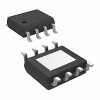
IC OPAMP DUAL HS HI OUTP 8-PSOP
Manufacturer
National Semiconductor
Series
VIP™ IIIr
Datasheet
1.LM7372IMANOPB.pdf
(16 pages)
Specifications of LM7372MR/NOPB
Amplifier Type
Voltage Feedback
Number Of Circuits
2
Slew Rate
3000 V/µs
Gain Bandwidth Product
120MHz
-3db Bandwidth
220MHz
Current - Input Bias
2.7µA
Voltage - Input Offset
2000µV
Current - Supply
13mA
Current - Output / Channel
260mA
Voltage - Supply, Single/dual (±)
9 V ~ 36 V, ±4.5 V ~ 18 V
Operating Temperature
-40°C ~ 85°C
Mounting Type
Surface Mount
Package / Case
8-PSOP
Lead Free Status / RoHS Status
Lead free / RoHS Compliant
Output Type
-
Other names
*LM7372MR
*LM7372MR/NOPB
LM7372MR
*LM7372MR/NOPB
LM7372MR


www.national.com
here with ample board copper area to aid in heat dissipation
(see table 2).
For most standard surface mount packages, 8-Pin SOIC, 14-
Pin SOIC, 16-Pin SOIC etc, the only means of heat removal
from the die is through the bond wires to external copper con-
necting to the leads. Usually it will be difficult to reduce the
thermal resistance of these packages below 100°C/W by
these methods and several manufacturers, including Nation-
al, offer package modifications to enhance the thermal char-
acteristics.
The LM7372 is available in the 16-Pin SOIC package. Since
only 8 pins are needed for the two operational amplifiers, the
remaining pins are used for heat sink purposes. Each of the
end pins, 1,8,9 & 16 are internally bonded to the lead frame
and form an effective means of transferring heat to external
copper. This external copper can be either electrically isolated
or be part of the topside ground plane in a single supply ap-
plication.
Figure 2. shows a copper pattern which can be used to dis-
sipate internal heat from the LM7372. Table 1 gives some
values of θ
From Table 1 it is apparent that two areas of 1oz copper at
each end of the package, each 2 in
2600mm
temperature under 120°C with an 85°C ambient temperature.
An even better package for removing internally generated
heat is a package with an exposed die attach paddle. Im-
proved removal of internal heat can be achieved by directly
connecting bond wires to the lead frame inside the package.
Since this lead frame supports the die attach paddle, heat is
transferred directly from the substrate to the outside copper
by these bond wires. The LM7372 is also available in the 8-
Pin PSOP package. For this package the entire lower surface
of the paddle is not covered with plastic, which would other-
wise act as a thermal barrier to heat transfer. Heat is trans-
ferred directly from the die through the paddle rather than
TABLE 1. 16-Pin SOIC Thermal Resistance with Area of
L (in)
2
1
2
3
) will be sufficient to hold the maximum junction
FIGURE 2. Copper Heatsink Patterns
JA
for different values of L and H with 1oz copper.
H (in)
Cu
0.5
1.5
1
2
in area (for a total of
θ
JA
20004925
(°C/W)
83
70
67
12
through the small diameter bonding wires. Values of θ
C/W for the PSOP package with various areas and weights
of copper are tabulated below.
Table 2 clearly demonstrates the superior thermal qualities of
the exposed pad package. For example, using the topside
copper only in the same way as shown for the SOIC package
(Figure 2), the PSOP requires half the area of 1 oz copper (2
in
of 72°C/Watt. This gives considerably more flexibility in the
pcb layout aside from using less copper.
The shape of the heat sink shown in Figure 2 is necessary to
allow external components to be connected to the package
pins. If thermal vias are used beneath the PSOP to the bottom
side ground plane, then a square pattern heat sink can be
used and there is no restriction on component placement on
the top side of the board. Even better thermal characteristics
are obtained with bottom layer heat sinking. A 2 inch square
of 0.5oz copper gives the same thermal resistance (81°C/W)
as a competitive thermally enhanced 8-Pin SOIC package
which needs two layers of 2 oz copper, each 4 in
of 5000 mm
low as 54°C/W are possible with bottom side heat sinking on-
ly, substantially improving the long term reliability since the
maximum junction temperature is held to less than 110°C,
even with an ambient temperature of 85°C. If both top and
bottom copper planes are used, the thermal resistance can
be brought to under 40°C/W.
HIGH FREQUENCY/LARGE SIGNAL SWING
CONSIDERATIONS
The LM7372 employs a unique input stage in order to support
large slew rate and high output current capability with large
output swings, with a relatively low quiescent current. This
input architecture boosts the device supply current when the
application demands it. The result is a supply current which
increases at high enough frequencies when the output swing
is large enough with added power dissipation as a conse-
quence.
Figure 3 shows the amount of increase in supply current as a
function of frequency for various sinusoidal output swing am-
plitudes:
2
Copper
, total or 1300mm
0.5 oz
1.0 oz
2.0 oz
0.5 oz
1.0 oz
2.0 oz
0.5 oz
1.0 oz
2.0 oz
TABLE 2. Thermal Resistance of PSOP Package
2
). With heavier copper, thermal resistances as
Top And
Bottom
Bottom
Layer
Layer
Area
Only
Only
Top
2
), for a comparable thermal resistance
0.5 in
(each
side)
115
102
91
74
92
85
83
71
63
2
1.0 in
(each
side)
105
79
60
88
75
66
70
57
48
2
2
(for a total
2.0 in
(each
side)
102
72
52
81
65
54
63
47
37
JA
2
in °
Related parts for LM7372MR/NOPB
Image
Part Number
Description
Manufacturer
Datasheet
Request
R

Part Number:
Description:
Operational Amplifier (Op-Amp) IC
Manufacturer:
National Semiconductor
Datasheet:

Part Number:
Description:
National Semiconductor [8-Bit D/A Converter]
Manufacturer:
National Semiconductor
Datasheet:
Part Number:
Description:
National Semiconductor [Media Coprocessor]
Manufacturer:
National Semiconductor
Datasheet:
Part Number:
Description:
Digitally Controlled Tone and Volume Circuit with Stereo Audio Power Amplifier, Microphone Preamp Stage and National 3D Sound
Manufacturer:
National Semiconductor
Datasheet:
Part Number:
Description:
Digitally Controlled Tone and Volume Circuit with Stereo Audio Power Amplifier, Microphone Preamp Stage and National 3D Sound
Manufacturer:
National Semiconductor
Datasheet:
Part Number:
Description:
AC97 Rev 2 Codec with Sample Rate Conversion and National 3D Sound
Manufacturer:
National Semiconductor
Part Number:
Description:
Manufacturer:
National Semiconductor
Datasheet:
Part Number:
Description:
Manufacturer:
National Semiconductor
Datasheet:
Part Number:
Description:
General Purpose, Low Voltage, Low Power, Rail-to-Rail Output Operational Amplifiers
Manufacturer:
National Semiconductor
Datasheet:
Part Number:
Description:
8-bit 20 MSPS flash A/D converter.
Manufacturer:
National Semiconductor
Datasheet:
Part Number:
Description:
Low Noise Quad Operational Amplifier
Manufacturer:
National Semiconductor
Datasheet:
Part Number:
Description:
Quad Differential Line Receivers
Manufacturer:
National Semiconductor
Datasheet:
Part Number:
Description:
Quad High Speed Trapezoidal? Bus Transceiver
Manufacturer:
National Semiconductor
Datasheet:
Part Number:
Description:
Dual Line Receiver
Manufacturer:
National Semiconductor
Datasheet: