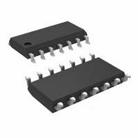
LMH6503MA/NOPB National Semiconductor, LMH6503MA/NOPB Datasheet - Page 16

LMH6503MA/NOPB
Manufacturer Part Number
LMH6503MA/NOPB
Description
IC AMP VARIABLE GAIN 14-SOIC
Manufacturer
National Semiconductor
Series
LMH®r
Datasheet
1.LMH6503MANOPB.pdf
(20 pages)
Specifications of LMH6503MA/NOPB
Amplifier Type
Variable Gain
Number Of Circuits
1
Slew Rate
1800 V/µs
-3db Bandwidth
135MHz
Current - Input Bias
11µA
Current - Supply
37mA
Current - Output / Channel
90mA
Voltage - Supply, Single/dual (±)
5 V ~ 12 V, ±2.5 V ~ 6 V
Operating Temperature
-40°C ~ 85°C
Mounting Type
Surface Mount
Package / Case
14-SOIC (3.9mm Width), 14-SOL
For Use With
CLC730033 - EVAL BOARD AMP FOR 14-SOIC
Lead Free Status / RoHS Status
Lead free / RoHS Compliant
Output Type
-
Gain Bandwidth Product
-
Voltage - Input Offset
-
Other names
*LMH6503MA
LMH6503MA
LMH6503MA
www.national.com
Application Information
NOISE
Figure 5 describes the LMH6503’s output-referred spot
noise density as a function of frequency with A
The plot includes all the noise contributing terms. However,
with both inputs terminated in 50Ω, the input noise contribu-
tion is minimal. At A
flat-band input-referred spot noise density (e
flat-band region, the input RMS voltage noise can be deter-
mined from the following single-pole model:
CIRCUIT LAYOUT CONSIDERATIONS
Good high-frequency operation requires all of the de-
coupling capacitors shown in Figure 6 to be placed as close
as possible to the power supply pins in order to insure a
proper high-frequency low-impedance bypass. Adequate
ground plane and low inductive power returns are also
FIGURE 6. Required Power Supply Decoupling
. For applications with −3dB BW extending well into the
FIGURE 5. Output Referred Voltage Noise vs.
VMAX
Frequency
= 10V/V, the LMH6503 has a typical
(Continued)
VMAX
20073957
in
) of 6.6nV/
20073922
= 10V/V.
(7)
16
required of the layout. Minimizing the parasitic capacitances
at pins 3, 4, 5, 6, 9, 10 and 12 will assure best high frequency
performance. The parasitic inductance of component leads
or traces to pins 4, 5 and 9 should also be kept to a
minimum. Parasitic or load capacitance, C
(pin 10) degrades phase margin and can lead to frequency
response peaking or circuit oscillation. The LMH6503 is fully
stable when driving a 100Ω load. With reduced load (e.g.
1kΩ) there is a possibility of instability at very high frequen-
cies beyond 400MHz especially with a capacitive load.
When the LMH6503 is connected to a light load as such, it is
recommended to add a snubber network to the output (e.g.
100Ω and 39pF in series tied between the LMH6503 output
and ground). C
placing a small resistor in series with the output (pin 10).
Component parasitics also influence high frequency results.
Therefore it is recommended to use metal film resistors such
as RN55D or leadless components such as surface mount
devices. High profile sockets are not recommended.
National Semiconductor suggests the following evaluation
board as a guide for high frequency layout and as an aid in
device testing and characterization:
The evaluation board is shipped when a device sample
request is placed with National Semiconductor.
SINGLE SUPPLY OPERATION
It is possible to operate the LMH6503 with a single supply. To
do so, tie pin 11 (GND) to a potential about mid point
between V
Figure 8.
Device
LMH6503MA
LMH6503MT
FIGURE 7. AC Coupled Single Supply VGA
+
and V
L
Package
SOIC-14
TSSOP-14
can also be isolated from the output by
−
. Two examples are shown in Figure 7 &
Evaluation Board Part
Number
CLC730033
CLC730146
L
, on the output
20073935


