LMH6503MA National Semiconductor, LMH6503MA Datasheet
LMH6503MA
Specifications of LMH6503MA
Available stocks


Related parts for LMH6503MA

LMH6503MA Summary of contents
Page 1
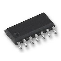
... For linear in dB gain control applications, see LMH6502 datasheet. The LMH6503 is available in the SOIC-14 and TSSOP-14 package. Gain vs. V for Various Temperature G LMH is a trademark of National Semiconductor Corporation. ™ © 2004 National Semiconductor Corporation Features ± 5V 25˚ ...
Page 2
... Absolute Maximum Ratings If Military/Aerospace specified devices are required, please contact the National Semiconductor Sales Office/ Distributors for availability and specifications. ESD Tolerance: (Note 4) Human Body Machine Model Input Current V Differential IN Output Current + − Supply Voltages ( Voltage at Input/ Output pins Soldering Information: ...
Page 3
Electrical Characteristics Unless otherwise specified, all limits guaranteed for T ± = 0.1V 100Ω +1V. Boldface limits apply at the temperature extremes. _DIFF L G Symbol Parameter DC & Miscellaneous Performance GACCU Gain Accuracy (see Application ...
Page 4
... < gain. For example, for f 30MHz, here are the Flat Band Attenuation ranges: 14-Pin SOIC/TSSOP 20073946 Top View Package Marking LMH6503MA LMH6503MT 4 is the change in output voltage with OUT 20073932 Transport Media NSC Drawing 55 Units/Rail 2.5k Units Tape and Reel 94 Units/Rail 2.5k Units Tape and Reel > ...
Page 5
Typical Performance Charateristics = 0V 1kΩ 174Ω, both inputs terminated in 50Ω Small Signal Frequency Response (A Frequency Response over Temperature (A Frequency Response for Various V ± ( 2.5V) Unless otherwise specified: ...
Page 6
Typical Performance Charateristics = 0V 1kΩ 174Ω, both inputs terminated in 50Ω output: (Continued) Large Signal Frequency Response Frequency Response for Various V (Large Signal www.national.com Unless otherwise ...
Page 7
Typical Performance Charateristics = 0V 1kΩ 174Ω, both inputs terminated in 50Ω output: (Continued) Input Bias Current vs. V ± PSRR 5V ± CMRR 5V Unless otherwise specified 100Ω, Typical values, ...
Page 8
Typical Performance Charateristics = 0V 1kΩ 174Ω, both inputs terminated in 50Ω output: (Continued) A vs. V VMAX Supply Current vs. V Output Offset Voltage vs.V CM www.national.com Unless otherwise specified ...
Page 9
Typical Performance Charateristics = 0V 1kΩ 174Ω, both inputs terminated in 50Ω output: (Continued) Output Offset Voltage vs.V CM Gain Flatness and Linear Phase Deviation Group Delay vs. Frequency Unless otherwise specified: V ...
Page 10
Typical Performance Charateristics = 0V 1kΩ 174Ω, both inputs terminated in 50Ω output: (Continued) Gain vs. V Including Limits G ± Gain vs Output Offset Voltage vs. V www.national.com Unless ...
Page 11
Typical Performance Charateristics = 0V 1kΩ 174Ω, both inputs terminated in 50Ω output: (Continued) ± Output Offset Voltage vs (Typical Unit 1) ± Output Offset Voltage vs (Typical Unit ...
Page 12
Typical Performance Charateristics = 0V 1kΩ 174Ω, both inputs terminated in 50Ω output: (Continued) Noise vs. Frequency (A Output Voltage vs. Output Current HD3 vs. P OUT www.national.com Unless otherwise specified ...
Page 13
Typical Performance Charateristics = 0V 1kΩ 174Ω, both inputs terminated in 50Ω output: (Continued) HD2 & HD3 vs Bias Current vs Step Response Plot Unless otherwise specified ...
Page 14
Typical Performance Charateristics = 0V 1kΩ 174Ω, both inputs terminated in 50Ω output: (Continued) Application Information THEORY OF OPERATION The LMH6503 is a linear wideband variable-gain amplifier as illustrated in Figure 1. A ...
Page 15
Application Information the minimum possible values that meet the input voltage and maximum gain constraints. Scaling the resistor values will decrease bandwidth and improve stability. Figure 2 illustrates the resulting LMH6503 bandwidths as a function of the maximum ( y ...
Page 16
... High profile sockets are not recommended. National Semiconductor suggests the following evaluation board as a guide for high frequency layout and as an aid in device testing and characterization: Device LMH6503MA LMH6503MT The evaluation board is shipped when a device sample request is placed with National Semiconductor. SINGLE SUPPLY OPERATION It is possible to operate the LMH6503 with a single supply ...
Page 17
Application Information FIGURE 8. Transformer Coupled Single Supply VGA OPERATING AT LOWER SUPPLY VOLTAGES The LMH6503 is rated for operation down to 5V supplies (V − There are some specifications shown for operation at ± 2.5V within ...
Page 18
Application Circuits FOUR-QUADRANT MULTIPLIER Applications requiring multiplication, squaring or other non- linear functions can be implemented with four-quadrant mul- tipliers. The LMH6503 implements a four-quadrant multiplier as illustrated in Figure 11: FIGURE 11. Four Quadrant Multiplier FREQUENCY SHAPING Frequency shaping ...
Page 19
Physical Dimensions inches (millimeters) unless otherwise noted 14-Pin SOIC NS Package Number M14A 14-Pin TSSOP NS Package Number MTC14 19 www.national.com ...
Page 20
... BANNED SUBSTANCE COMPLIANCE National Semiconductor certifies that the products and packing materials meet the provisions of the Customer Products Stewardship Specification (CSP-9-111C2) and the Banned Substances and Materials of Interest Specification (CSP-9-111S2) and contain no ‘‘Banned Substances’’ as defined in CSP-9-111S2. ...