LMH6502MA/NOPB National Semiconductor, LMH6502MA/NOPB Datasheet - Page 14

LMH6502MA/NOPB
Manufacturer Part Number
LMH6502MA/NOPB
Description
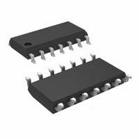
IC AMP VARIABLE GAIN 14-SOIC
Manufacturer
National Semiconductor
Series
LMH®r
Type
Variable Gain Amplifierr
Datasheet
1.LMH6502MANOPB.pdf
(19 pages)
Specifications of LMH6502MA/NOPB
Amplifier Type
Variable Gain
Number Of Circuits
1
Slew Rate
1800 V/µs
-3db Bandwidth
130MHz
Current - Input Bias
9µA
Current - Supply
27mA
Current - Output / Channel
90mA
Voltage - Supply, Single/dual (±)
5 V ~ 12 V, ±2.5 V ~ 6 V
Operating Temperature
-40°C ~ 85°C
Mounting Type
Surface Mount
Package / Case
14-SOIC (3.9mm Width), 14-SOL
Number Of Channels
1
Number Of Elements
1
Power Supply Requirement
Single/Dual
Common Mode Rejection Ratio
72dB
Unity Gain Bandwidth Product (typ)
100MHz
Single Supply Voltage (typ)
9V
Dual Supply Voltage (typ)
±3/±5V
Power Supply Rejection Ratio
69dB
Rail/rail I/o Type
No
Single Supply Voltage (min)
5V
Single Supply Voltage (max)
12V
Dual Supply Voltage (min)
±2.5V
Dual Supply Voltage (max)
±6V
Operating Temp Range
-40C to 85C
Operating Temperature Classification
Industrial
Mounting
Surface Mount
Pin Count
14
Package Type
SOIC N
For Use With
CLC730033 - EVAL BOARD AMP FOR 14-SOIC
Lead Free Status / RoHS Status
Lead free / RoHS Compliant
Output Type
-
Gain Bandwidth Product
-
Voltage - Input Offset
-
Lead Free Status / Rohs Status
Compliant
Other names
*LMH6502MA
*LMH6502MA/NOPB
LMH6502MA
*LMH6502MA/NOPB
LMH6502MA
Available stocks
Company
Part Number
Manufacturer
Quantity
Price
Part Number:
LMH6502MA/NOPB
Manufacturer:
NS/国半
Quantity:
20 000
www.national.com
Typical Performance Characteristics
output. (Continued)
Application Information
THEORY OF OPERATION
A simplified schematic is shown in Figure 1. +V
are buffered with closed loop voltage followers inducing a
signal current in Rg proportional to (+V
ferential input voltage. This current controls a current source
which supplies two well-matched transistor, Q1 and Q2.
The current flowing through Q2 is converted to the final
output voltage using R
changing the fraction of the signal current "I" which flows
through Q2, the gain is changed. This is done by changing
the voltage applied differentially to the bases of Q1 and Q2.
For example, with V
off. With none of "I" flowing through R
to output gain is strongly attenuated. With V
and the entire signal current flows through Q2 to R
ing maximum gain. With V
Q2 are set to approximately the same voltage, Q1 and Q2
have the same collector currents - equal to one half of the
signal current "I", thus the gain is approximately one half the
maximum gain.
= 0V, R
F
= 1kΩ, R
FIGURE 1. LMH6502 Block Diagram
G
G
= 174Ω, both inputs terminated in 50Ω, R
= 0V, Q1 conducts heavily and Q2 is
F
and the output amplifier, U1. By
G
set to 1V, the bases of Q1 and
F
, the LMH6502’s input
IN
) - (−V
G
= +2V, Q1 is off
IN
IN
), the dif-
F
and −V
Feedthrough from V
produc-
20067741
IN
Unless otherwise specified: V
14
L
= 100Ω, Typical values, results referred to device
CHOOSING R
Maximum input amplitude and maximum gain are the two
key specifications that determine component values in a
LMH6502 application.
The output stage op amp is a current-feedback type amplifier
optimized for R
To determine whether the maximum input amplitude will
overdrive the LMH6502, compute:
the maximum differential input voltage for linear operation. If
the maximum input amplitude exceeds the above V
limit, then LMH6502 should either be moved to a location in
the signal chain where input amplitudes are reduced, or the
LMH6502 gain A
R
mance impact is different based on the choice made. If the
input amplitude is reduced, re-compute the impact on signal-
to-noise ratio. If A
gain, should be increased, or another gain stage added to
make up for reduced system gain. To increase R
compute the lowest acceptable value for R
Operating with R
eration of the input buffers.
R
should be
<
reducing resistor to ground on the inverting summing node of
the output amplifier (see application note QA-13 for details).
ADJUSTING OFFSET
Offset can be broken into two parts; an input-referred term
and an output-referred term. The input-referred offset shows
up as a variation in output voltage as V
can be trimmed using the circuit in Figure 2 by placing a low
frequency square wave (V
G
F
1kΩ can be implemented if necessary using a loop gain
and R
may be computed from selected R
G
F
>
should be increased. The overall system perfor-
= 1kΩ for overall best performance, however R
V
F
F
DMAX
20067765
& R
VMAX
= 1kΩ. R
G
R
VMAX
G
larger than this value insures linear op-
G
= (R
>
should be reduced or the values for
is reduced, post LMH6502 amplifier
590 x V
S
G
LOW
G
=
+ 3.0Ω) x 1.70mA
can then be computed as:
±
5V, 25˚C, V
= 0V, V
DMAX
- 3Ω
HIGH
G
G
G
= 2V into V
is changed. This
G
and A
:
= V
GMAX
G
VMAX
and R
, V
G
DMAX
: R
with
CM
(1)
(2)
(3)
F
F
F
,


