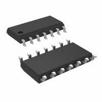
LMH6502MA/NOPB National Semiconductor, LMH6502MA/NOPB Datasheet - Page 16

LMH6502MA/NOPB
Manufacturer Part Number
LMH6502MA/NOPB
Description
IC AMP VARIABLE GAIN 14-SOIC
Manufacturer
National Semiconductor
Series
LMH®r
Type
Variable Gain Amplifierr
Datasheet
1.LMH6502MANOPB.pdf
(19 pages)
Specifications of LMH6502MA/NOPB
Amplifier Type
Variable Gain
Number Of Circuits
1
Slew Rate
1800 V/µs
-3db Bandwidth
130MHz
Current - Input Bias
9µA
Current - Supply
27mA
Current - Output / Channel
90mA
Voltage - Supply, Single/dual (±)
5 V ~ 12 V, ±2.5 V ~ 6 V
Operating Temperature
-40°C ~ 85°C
Mounting Type
Surface Mount
Package / Case
14-SOIC (3.9mm Width), 14-SOL
Number Of Channels
1
Number Of Elements
1
Power Supply Requirement
Single/Dual
Common Mode Rejection Ratio
72dB
Unity Gain Bandwidth Product (typ)
100MHz
Single Supply Voltage (typ)
9V
Dual Supply Voltage (typ)
±3/±5V
Power Supply Rejection Ratio
69dB
Rail/rail I/o Type
No
Single Supply Voltage (min)
5V
Single Supply Voltage (max)
12V
Dual Supply Voltage (min)
±2.5V
Dual Supply Voltage (max)
±6V
Operating Temp Range
-40C to 85C
Operating Temperature Classification
Industrial
Mounting
Surface Mount
Pin Count
14
Package Type
SOIC N
For Use With
CLC730033 - EVAL BOARD AMP FOR 14-SOIC
Lead Free Status / RoHS Status
Lead free / RoHS Compliant
Output Type
-
Gain Bandwidth Product
-
Voltage - Input Offset
-
Lead Free Status / Rohs Status
Compliant
Other names
*LMH6502MA
*LMH6502MA/NOPB
LMH6502MA
*LMH6502MA/NOPB
LMH6502MA
Available stocks
Company
Part Number
Manufacturer
Quantity
Price
Part Number:
LMH6502MA/NOPB
Manufacturer:
NS/国半
Quantity:
20 000
www.national.com
Application Information
National Semiconductor suggests the following evaluation
boards as a guide for high frequency layout and as an aid in
device testing and characterization:
The evaluation board is shipped when a device sample
request is placed with National Semiconductor
SINGLE SUPPLY OPERATION
It is possible to operate the LMH6502 with a single supply. To
do so, tie pin 11 (GND) to a potential about mid point
between V
Figure 5.
Device
LMH6502MA
LMH6502MT
FIGURE 5. Transformer Coupled Single Supply VGA
FIGURE 4. AC Coupled Single Supply VGA
+
and V
Package
SOIC-14
TSSOP-14
−
. Two examples are shown in Figure 4 &
Evaluation Board
Part Number
CLC730033
CLC730146
(Continued)
20067747
20067746
16
OPERATING AT LOWER SUPPLY VOLTAGES
The LMH6502 is rated for operation down to 5V supplies (V
-V
±
CMRR, PSRR, Gain vs. V
tion, at lower supplies:
a) V
b) V
c) "Max_gain" reduces. There is an intrinsic reduction in
Application Circuits
AGC LOOP
Figure 6 shows a typical AGC circuit. The LMH6502 is
followed up with a LMH6714 for higher overall gain. The
output of the LMH6714 is rectified and fed to an inverting
integrator using a LMH6657 (wideband voltage feedback op
amp). When the output voltage, V
grator output voltage ramps down reducing the net gain of
the LMH6502 and V
the integrator ramps up increasing the net gain and the
output voltage. Actual output level is set with R
shifts in DC output voltage with DC changes in input signal
level, trim pot R
in the range of input signals over which constant output level
can be maintained. In this circuit, we would expect that
reasonable AGC action could be maintained for at least
40dB. In practice, rectifier dynamic range limits reduce this
slightly.
V
V
V
V
2.5V within the data sheet (i.e. Frequency Response,
−
G
G_MIN
G_MID
G_MAX
). There are some specifications shown for operation at
Here are the approximate expressions for various V
voltages as a function of V
duced. This is due to limitations within the device arising
from transistor headroom. Beyond this limit, device per-
formance will be affected (non-destructive). This could
reveal itself as premature high frequency response roll-
off. With
V
that operating under these conditions has reduced the
maximum permissible voltage on V
what is needed to get Max gain. If supply voltages are
asymmetrical with V
V
= −3V, V
being 2.5dB less than what would be expected when V
is higher.
max gain when the total supply voltage is reduced (see
Typical Performance Characteristics plots for Gain vs. V
(V
mechanism described in "b" above. Beyond V
high frequency response is also effected.
G
G_LIMIT
G
G
S
range could result; for example, with V
range shifts lower.
= 1.5V is needed to get maximum gain. This means
=
TABLE 1. V
±
±
G_LIMIT
2.5V). In addition, there is the more drastic
(maximum permissible voltage on V
2.5V supplies, V
2
is provided. AGC circuits are always limited
Definition
Gain Cut-off
A
A
VMAX
VMAX
= 0.40V which results in maximum gain
OUT
G
+
. If the output voltage is too small,
Definition Based on V
/2
being lower, further "pinching" of
G
, etc.). Compared to
G_LIMIT
+
:
OUT
is below 1.1V whereas
, is too large the inte-
G
Expression (V)
0.2 x V
0.2 x V
0.2 x V
to a level below
+
= 2V, and V
1
+
+
+
. To prevent
±
+
−1
+1
5V opera-
G
) is re-
G_LIMIT
G
G
S
+
−
,


