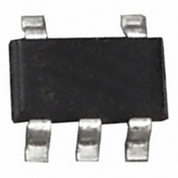
EL5165IW-T7 Intersil, EL5165IW-T7 Datasheet - Page 10

EL5165IW-T7
Manufacturer Part Number
EL5165IW-T7
Description
IC OP AMP 600MHZ CURR FB SOT23-5
Manufacturer
Intersil
Datasheet
1.EL5164ISZ.pdf
(16 pages)
Specifications of EL5165IW-T7
Amplifier Type
Current Feedback
Number Of Circuits
1
Slew Rate
4700 V/µs
-3db Bandwidth
600MHz
Current - Input Bias
2µA
Voltage - Input Offset
1500µV
Current - Supply
3.5mA
Current - Output / Channel
190mA
Voltage - Supply, Single/dual (±)
5 V ~ 12 V, ±2.5 V ~ 6 V
Operating Temperature
-40°C ~ 85°C
Mounting Type
Surface Mount
Package / Case
SOT-23-5, SC-74A, SOT-25
Lead Free Status / RoHS Status
Contains lead / RoHS non-compliant
Output Type
-
Gain Bandwidth Product
-
Other names
EL5165IW-T7TR
inductance. Use of sockets, particularly for the SO package,
should be avoided if possible. Sockets add parasitic
inductance and capacitance which will result in additional
peaking and overshoot.
Disable/Power-Down
The EL5164 amplifier can be disabled placing its output in a
high impedance state. When disabled, the amplifier supply
current is reduced to <150µA. The EL5164 is disabled when
its CE pin is pulled up to within 1V of the positive supply.
Similarly, the amplifier is enabled by floating or pulling its CE
pin to at least 3V below the positive supply. For ±5V supply,
this means that an EL5164 amplifier will be enabled when
CE is 2V or less, and disabled when CE is above 4V.
Although the logic levels are not standard TTL, this choice of
logic voltages allows the EL5164 to be enabled by tying CE
to ground, even in 5V single supply applications. The CE pin
can be driven from CMOS outputs.
When the amplifier is disabled, if the positive input is driven
beyond ±2V with respect to the negative input, the device
can become active and output the signal. An input diode
clamp network D
used to keep the device disabled while a large input signal is
present.
Capacitance at the Inverting Input
Any manufacturer’s high-speed voltage- or current-feedback
amplifier can be affected by stray capacitance at the
inverting input. For inverting gains, this parasitic capacitance
has little effect because the inverting input is a virtual
ground, but for non-inverting gains, this capacitance (in
conjunction with the feedback and gain resistors) creates a
pole in the feedback path of the amplifier. This pole, if low
enough in frequency, has the same destabilizing effect as a
zero in the forward open-loop response. The use of large-
value feedback and gain resistors exacerbates the problem
by further lowering the pole frequency (increasing the
possibility of oscillation.)
The EL5164, EL5165, and EL5364 have been optimized
with a 510Ω feedback resistor. With the high bandwidth of
these amplifiers, these resistor values might cause stability
problems when combined with parasitic capacitance, thus
ground plane is not recommended around the inverting input
pin of the amplifier.
V
IN
FIGURE 23. DISABLED AMPLIFIER
1
R
and D
G
D
1
2
, as shown in Figure 23, can be
10
R
D
F
2
-
+
+5V
-5V
CE
+5V
EL5164, EL5165, EL5364
V
OUT
Feedback Resistor Values
The EL5164, EL5165, and EL5364 have been designed and
specified at a gain of +2 with R
value of feedback resistor gives 300MHz of -3dB bandwidth
at A
gives 275MHz of bandwidth with 1dB of peaking. Since the
EL5164, EL5165, and EL5364 are current-feedback
amplifiers, it is also possible to change the value of R
more bandwidth. As seen in the curve of Frequency
Response for Various R
can be easily modified by varying the value of the feedback
resistor.
Because the EL5164, EL5165, and EL5364 are
current-feedback amplifiers, their gain-bandwidth product is
not a constant for different closed-loop gains. This feature
actually allows the EL5164, EL5165, and EL5364 to
maintain about the same -3dB bandwidth. As gain is
increased, bandwidth decreases slightly while stability
increases. Since the loop stability is improving with higher
closed-loop gains, it becomes possible to reduce the value
of R
resulting in only a slight loss of bandwidth with increased
closed-loop gain.
Supply Voltage Range and Single-Supply
Operation
The EL5164, EL5165, and EL5364 have been designed to
operate with supply voltages having a span of greater than
5V and less than 10V. In practical terms, this means that
they will operate on dual supplies ranging from ±2.5V to ±5V.
With single-supply, the EL5164, EL5165, and EL5364 will
operate from 5V to 10V.
As supply voltages continue to decrease, it becomes
necessary to provide input and output voltage ranges that
can get as close as possible to the supply voltages. The
EL5164, EL5165, and EL5364 have an input range which
extends to within 2V of either supply. So, for example, on
±5V supplies, the EL5164, EL5165, and EL5364 have an
input range which spans ±3V. The output range of the
EL5164, EL5165, and EL5364 is also quite large, extending
to within 1V of the supply rail. On a ±5V supply, the output is
therefore capable of swinging from -4V to +4V. Single-supply
output range is larger because of the increased negative
swing due to the external pull-down resistor to ground.
Video Performance
For good video performance, an amplifier is required to
maintain the same output impedance and the same frequency
response as DC levels are changed at the output. This is
especially difficult when driving a standard video load of 150Ω,
because of the change in output current with DC level.
Previously, good differential gain could only be achieved by
running high idle currents through the output transistors (to
reduce variations in output impedance.) These currents were
typically comparable to the entire 5.5mA supply current of
V
F
= 2 with 2dB of peaking. With A
below the specified 160Ω and still retain stability,
F
and R
F
G
approximately 412Ω. This
, bandwidth and peaking
V
= -2, an R
October 29, 2007
F
of 300Ω
F
FN7389.8
to get


