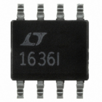
LT1636IS8 Linear Technology, LT1636IS8 Datasheet - Page 11

LT1636IS8
Manufacturer Part Number
LT1636IS8
Description
IC OPAMP R-R IN/OUT 220KHZ 8SOIC
Manufacturer
Linear Technology
Series
Over-The-Top®r
Datasheet
1.LT1636CN8PBF.pdf
(16 pages)
Specifications of LT1636IS8
Amplifier Type
General Purpose
Number Of Circuits
1
Output Type
Rail-to-Rail
Slew Rate
0.075 V/µs
Gain Bandwidth Product
220kHz
Current - Input Bias
4nA
Voltage - Input Offset
100µV
Current - Supply
50µA
Current - Output / Channel
30mA
Voltage - Supply, Single/dual (±)
2.7 V ~ 44 V, ±1.35 V ~ 22 V
Operating Temperature
-40°C ~ 85°C
Mounting Type
Surface Mount
Package / Case
8-SOIC (3.9mm Width)
Lead Free Status / RoHS Status
Contains lead / RoHS non-compliant
-3db Bandwidth
-
Available stocks
Company
Part Number
Manufacturer
Quantity
Price
Part Number:
LT1636IS8
Manufacturer:
LINEAR/凌特
Quantity:
20 000
Company:
Part Number:
LT1636IS8#PBF
Manufacturer:
TI
Quantity:
753
Company:
Part Number:
LT1636IS8#TRPBF
Manufacturer:
LINEAR
Quantity:
7 801
Part Number:
LT1636IS8#TRPBF
Manufacturer:
LINAR
Quantity:
20 000
APPLICATIONS
The normally reverse biased substrate diode from the
output to V
output is forced below V
limited to 100mA, no damage will occur.
The LT1636 is internally compensated to drive at least
200pF of capacitance under any output loading condi-
tions. A 0.22µF capacitor in series with a 150Ω resistor
between the output and ground will compensate these
amplifiers for larger capacitive loads, up to 10,000pF, at
all output currents.
Distortion
There are two main contributors of distortion in op amps:
output crossover distortion as the output transitions from
sourcing to sinking current and distortion caused by
nonlinear common mode rejection. Of course, if the op
amp is operating inverting there is no common mode
induced distortion. When the LT1636 switches between
input stages there is significant nonlinearity in the CMRR.
Lower load resistance increases the output crossover
distortion, but has no effect on the input stage transition
distortion. For lowest distortion the LT1636 should be
operated single supply, with the output always sourcing
current and with the input voltage swing between ground
and (V
istics curves.
Gain
The open-loop gain is less sensitive to load resistance
when the output is sourcing current. This optimizes per-
formance in single supply applications where the load is
+
– 0.8V). See the Typical Performance Character-
–
will cause unlimited currents to flow when the
U
INFORMATION
–
U
. If the current is transient and
W
U
returned to ground. The typical performance photo of
Open-Loop Gain for various loads shows the details.
Shutdown
The LT1636 can be shut down two ways: using the
shutdown pin or bringing V
is brought to within 0.5V of V
output leakage current drop to less than 1nA. When the
shutdown pin is brought 1.2V above V
current drops to about 4µA and the output leakage current
is less than 1µA, independent of V
bias current is less than 0.1nA (even if the inputs are 44V
above the negative supply).
The shutdown pin can be taken up to 32V above V
shutdown pin can be driven below V
current through the substrate diode should be limited with
an external resistor to less than 10mA.
Input Offset Nulling
The input offset voltage can be nulled by placing a 10k
potentiometer between Pins 1 and 8 with its wiper to V
(see Figure 1). The null range will be at least ±1mV.
Figure 1. Input Offset Nulling
LT1636
1
+
10k
V
to within 0.5V of V
–
–
both the supply current and
8
+
. In either case the input
1636 F01
–
, however the pin
–
, the supply
LT1636
–
. When V
11
–
. The
1636fc
+
–


