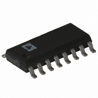
AD8594ARZ Analog Devices Inc, AD8594ARZ Datasheet - Page 10

AD8594ARZ
Manufacturer Part Number
AD8594ARZ
Description
IC OPAMP GP R-R CMOS 3MHZ 16SOIC
Manufacturer
Analog Devices Inc
Specifications of AD8594ARZ
Slew Rate
5 V/µs
Amplifier Type
General Purpose
Number Of Circuits
4
Output Type
Rail-to-Rail
Gain Bandwidth Product
3MHz
Current - Input Bias
5pA
Voltage - Input Offset
2000µV
Current - Supply
1.25mA
Current - Output / Channel
250mA
Voltage - Supply, Single/dual (±)
2.5 V ~ 6 V
Operating Temperature
-40°C ~ 85°C
Mounting Type
Surface Mount
Package / Case
16-SOIC (3.9mm Width)
Op Amp Type
Low Input Bias
No. Of Amplifiers
4
Bandwidth
3MHz
Supply Voltage Range
2.5V To 6V
Amplifier Case Style
SOIC
No. Of Pins
16
Operating Temperature Range
-40°C To
Lead Free Status / RoHS Status
Lead free / RoHS Compliant
-3db Bandwidth
-
Lead Free Status / RoHS Status
Lead free / RoHS Compliant, Lead free / RoHS Compliant
Available stocks
Company
Part Number
Manufacturer
Quantity
Price
Company:
Part Number:
AD8594ARZ
Manufacturer:
AVAGO
Quantity:
1 000
Part Number:
AD8594ARZ
Manufacturer:
ADI/亚德诺
Quantity:
20 000
AD8591/AD8592/AD8594
If gain is required from the output amplifier, four additional
resistors should be added as shown in Figure 35. The gain of
the AD8592 can be set as:
Figure 35. A PC-98 Compliant Headphone/Line Out
Amplifier With Gain
Input coupling capacitors are not required for either circuit as
the reference voltage is supplied from the AD1881.
R4 and R5 help protect the AD8592 output in case the output
jack or headphone wires accidentally get shorted to ground.
The output coupling capacitors C1 and C2 block dc current
from the headphones and create a high-pass filter with a corner
frequency of:
Where R
NOTE: ADDITIONAL PINS
OMITTED FOR CLARITY
AD1881
RIGHT
(AC97)
A
LEFT
f
V
–3
V
L
V
V
V
dB
OUT
OUT
REF
DD
DD
SS
is the resistance of the headphones.
R
R
36
6
38
35
27
7
2
10k
10k
+5V
R6
R6
C
1
2
3
7
8
R
1
5
6
U1-A
U1-B
4
20k
20k
R7
R7
+5V
A
10
V
R
4
=
L
100k
9
R7
R6
1
U1 = AD8592
R1
= +6dB WITH VALUES SHOWN
+5V
100 F
100 F
C1
C2
2k
2k
R2
R3
20
20
R4
R5
NC
(5)
(6)
–10–
A Combined Microphone and Speaker Amplifier for
Cellphone and Portable Headsets
The dual amplifiers in the AD8592 make an efficient design for
interfacing with a headset containing a microphone and speaker.
Figure 36 demonstrates a simple method for constructing an
interface to a codec.
U1-A is used as a microphone preamplifier, where the gain of
the preamplifier is set as R3/R2. R1 is used to bias an electret
microphone and C1 blocks any dc voltages from the amplifier.
U1-B is the speaker amplifier, and its gain is set at R5/R4. To
sum a stereo output, R6 should be added, equal in value to R4.
Using the same principle as described in the previous section,
the normalizing contact on the microphone/speaker jack can be
used to put the AD8592 into shutdown when the headset is not
plugged in. The AD8592 shutdown inputs can also be con-
trolled with TTL or CMOS compatible logic, allowing micro-
phone or speaker muting if desired.
An Inexpensive Sample-and-Hold Circuit
The independent shutdown control of each amplifier in the
AD8592 allows a degree of flexibility in circuit design. One par-
ticular application for which this feature is useful is in designing a
sample-and-hold circuit for data acquisition. Figure 37 shows a
schematic of a simple, yet extremely effective sample-and-hold
circuit using a single AD8592 and one capacitor.
MIC + SPEAKER
V
IN
Figure 36. A Speaker/Mic Headset Amplifier Circuit
JACK
Figure 37. An Efficient Sample-and-Hold Circuit
2
3
U1 = AD8592
1k
U1-A
SAMPLE
CLOCK
R7
2.2k
+5V
R1
10
5
+5V
NC
4
1
0.1 F
C1
100k
10 F
C2
R8
10k
+5V
C1
1nF
R2
8
7
9
U1 = AD8592
2
3
U1-B
10k
5
100k
U1-A
R5
U1-B
R3
6
6
+5V
10
+5V
4
9
7
8
1
(OPTIONAL)
10k
10k
R6
R4
SAMPLE
AND HOLD
OUTPUT
TO
CODEC
V
FROM CODEC
FROM CODEC
MONO OUT
(OR LEFT OUT)
(RIGHT OUT)
REF
REV. A


