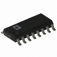
AD8594ARZ Analog Devices Inc, AD8594ARZ Datasheet - Page 12

AD8594ARZ
Manufacturer Part Number
AD8594ARZ
Description
IC OPAMP GP R-R CMOS 3MHZ 16SOIC
Manufacturer
Analog Devices Inc
Specifications of AD8594ARZ
Slew Rate
5 V/µs
Amplifier Type
General Purpose
Number Of Circuits
4
Output Type
Rail-to-Rail
Gain Bandwidth Product
3MHz
Current - Input Bias
5pA
Voltage - Input Offset
2000µV
Current - Supply
1.25mA
Current - Output / Channel
250mA
Voltage - Supply, Single/dual (±)
2.5 V ~ 6 V
Operating Temperature
-40°C ~ 85°C
Mounting Type
Surface Mount
Package / Case
16-SOIC (3.9mm Width)
Op Amp Type
Low Input Bias
No. Of Amplifiers
4
Bandwidth
3MHz
Supply Voltage Range
2.5V To 6V
Amplifier Case Style
SOIC
No. Of Pins
16
Operating Temperature Range
-40°C To
Lead Free Status / RoHS Status
Lead free / RoHS Compliant
-3db Bandwidth
-
Lead Free Status / RoHS Status
Lead free / RoHS Compliant, Lead free / RoHS Compliant
Available stocks
Company
Part Number
Manufacturer
Quantity
Price
Company:
Part Number:
AD8594ARZ
Manufacturer:
AVAGO
Quantity:
1 000
Part Number:
AD8594ARZ
Manufacturer:
ADI/亚德诺
Quantity:
20 000
AD8591/AD8592/AD8594
SPICE Model for the AD8591/AD8592/AD8594 Amplifier
The SPICE model for the AD8591/AD8592/AD8594 amplifier is
one of the more realistic computer simulation macro-models
available, providing a high degree of realism with respect to char-
acteristics of the actual amplifier. This model, shown in Listing 1,
is based on typical values for the device and can be downloaded
from Analog Devices’ Internet site at www.analog.com.
The model uses a common source output stage to provide rail-
to-rail performance. This allows realistic simulation of open-
loop gain dependency on load resistance as well as maximum
output voltage versus output current. Two differential pairs are
used in the input stage of the model, simulating the rail-to-rail
input stage of the AD8591/AD8592/AD8594 amplifier.
The EOS voltage source establishes the input offset voltage and
is also used to simulate the common-mode rejection power
supply rejection, and input voltage noise characteristics for the
model. In addition, G2, R2 and CF are used to help set the
open-loop gain and gain-bandwidth product of the model.
–12–
A number of secondary characteristics are also accurately por-
trayed in the SPICE model. Flicker noise is accurately modeled
with the 1/f corner frequency set through the KF and AF terms
in the input stage transistors. C1 and C2 are used in the input
section to create secondary poles to achieve an accurate phase
margin characteristic for the model.
The AD8591/AD8592/AD8594 shutdown circuitry is included
in the model. Switches S1 through S7 deactivate the op amp
circuitry in shutdown mode. The logic threshold for the shut-
down circuitry is accurately modeled through the VSWITCH
model parameters near the end of the listing. The active supply
current versus supply voltage is also modeled through the volt-
age-controlled current source GSY.
Characteristics of this model are based on typical values for the
AD8591/AD8592/AD8594 amplifier at +27 C. The model’s
characteristics are optimized specifically at +27 C, and may lose
accuracy at different simulation temperatures.
REV. A


