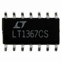
LT1367CS Linear Technology, LT1367CS Datasheet - Page 13

LT1367CS
Manufacturer Part Number
LT1367CS
Description
IC OP-AMP R-R IN/OUT QUAD 14SOIC
Manufacturer
Linear Technology
Datasheet
1.LT1368CN8PBF.pdf
(20 pages)
Specifications of LT1367CS
Amplifier Type
General Purpose
Number Of Circuits
4
Output Type
Rail-to-Rail
Slew Rate
0.13 V/µs
Gain Bandwidth Product
400kHz
Current - Input Bias
10nA
Voltage - Input Offset
200µV
Current - Supply
370µA
Current - Output / Channel
75mA
Voltage - Supply, Single/dual (±)
1.8 V ~ 30 V, ±0.9 V ~ 15 V
Operating Temperature
0°C ~ 70°C
Mounting Type
Surface Mount
Package / Case
14-SOIC (3.9mm Width), 14-SOL
Lead Free Status / RoHS Status
Contains lead / RoHS non-compliant
-3db Bandwidth
-
Available stocks
Company
Part Number
Manufacturer
Quantity
Price
Company:
Part Number:
LT1367CS
Manufacturer:
LT
Quantity:
5 510
Company:
Part Number:
LT1367CS
Manufacturer:
MAXIM
Quantity:
5 510
Part Number:
LT1367CS
Manufacturer:
LINEAR/凌特
Quantity:
20 000
Company:
Part Number:
LT1367CS#PBF
Manufacturer:
LT
Quantity:
1 269
Part Number:
LT1367CS#PBF
Manufacturer:
LINEAR/凌特
Quantity:
20 000
Company:
Part Number:
LT1367CS#TRPBF
Manufacturer:
LINEAR
Quantity:
17 023
Part Number:
LT1367CS#TRPBF
Manufacturer:
LINEAR/凌特
Quantity:
20 000
100mV/DIV
100mV/DIV
applicaTions inForMaTion
Improved Supply Rejection in the LT1368/LT1369
The LT1368/LT1369 are variations of the LT1366/LT1367
offering greater supply rejection and lower high frequency
output impedance. The LT1368/LT1369 require a 0.1µF load
capacitance for compensation. The output capacitance
forms a filter, which reduces pickup from the supply and
lowers the output impedance. This additional filtering is
helpful in mixed analog/digital systems with common sup-
plies, or systems employing switching supplies. Filtering
also reduces high frequency noise, which may be beneficial
when driving A/D converters.
Typical applicaTions
Buffering A/D Converters
Figure 5 shows the LT1368 driving an LTC
nel micropower A/D converter (ADC). The LTC1288 can
accommodate voltage references and input signals equal
to the supply rails. The sampling nature of this ADC
eliminates the need for an external sample-and-hold, but
may call for a drive amplifier because of the ADC’s 12µs
settling requirement. The LT1368’s rail-to-rail operation
and low input offset voltage make it well-suited for low
power, low frequency A/D applications. Either the LT1366
or LT1368 could be used for this application. However,
for low frequencies (f < 1kHz) the LT1368 provides better
supply rejection.
V
+
V
(AC)
OUT
Figure 4a. LT1366 Power Supply Rejection Test
2µs/DIV
®
1288 2-chan-
LT1366 F04a
Figure 4 shows the outputs of the LT1366/LT1368 perturbed
by a 200mV
supply. The LT1368’s power supply rejection is about ten
times greater than that of the LT1366 at 50kHz. Note the
5-to-1 scale change in the output voltage traces.
The tolerance of the external compensation capacitor is
not critical. The plots of Overshoot vs Load Current in the
Typical Performance Characteristics section illustrate the
effect of a capacitive load.
V
V
100mV/DIV
20mV/DIV
0
1
V
+
V
+
–
+
–
(AC)
1/2 LT1368
1/2 LT1368
OUT
Figure 4b. LT1368 Power Supply Rejection Test
Figure 5. 2-Channel Low Power A/D Converter
P-P
50kHz square wave added to the positive
0.1µF
0.1µF
0.1µF
2µs/DIV
LT1366/LT1367
LT1368/LT1369
V
CC
CS/SHDN
CH0
CH1
GND
LTC1288
V
CC
(REF)
D
LT1366 FO5
CLK
OUT
D
IN
1µF
LT1366 F04b
TO µP
1366fb


