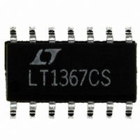
LT1367CS Linear Technology, LT1367CS Datasheet - Page 15

LT1367CS
Manufacturer Part Number
LT1367CS
Description
IC OP-AMP R-R IN/OUT QUAD 14SOIC
Manufacturer
Linear Technology
Datasheet
1.LT1368CN8PBF.pdf
(20 pages)
Specifications of LT1367CS
Amplifier Type
General Purpose
Number Of Circuits
4
Output Type
Rail-to-Rail
Slew Rate
0.13 V/µs
Gain Bandwidth Product
400kHz
Current - Input Bias
10nA
Voltage - Input Offset
200µV
Current - Supply
370µA
Current - Output / Channel
75mA
Voltage - Supply, Single/dual (±)
1.8 V ~ 30 V, ±0.9 V ~ 15 V
Operating Temperature
0°C ~ 70°C
Mounting Type
Surface Mount
Package / Case
14-SOIC (3.9mm Width), 14-SOL
Lead Free Status / RoHS Status
Contains lead / RoHS non-compliant
-3db Bandwidth
-
Available stocks
Company
Part Number
Manufacturer
Quantity
Price
Company:
Part Number:
LT1367CS
Manufacturer:
LT
Quantity:
5 510
Company:
Part Number:
LT1367CS
Manufacturer:
MAXIM
Quantity:
5 510
Part Number:
LT1367CS
Manufacturer:
LINEAR/凌特
Quantity:
20 000
Company:
Part Number:
LT1367CS#PBF
Manufacturer:
LT
Quantity:
1 269
Part Number:
LT1367CS#PBF
Manufacturer:
LINEAR/凌特
Quantity:
20 000
Company:
Part Number:
LT1367CS#TRPBF
Manufacturer:
LINEAR
Quantity:
17 023
Part Number:
LT1367CS#TRPBF
Manufacturer:
LINEAR/凌特
Quantity:
20 000
Typical applicaTions
High Side Current Source
The wide compliance current source shown in Figure 7
takes advantage of the LT1366’s ability to measure small
signals near the positive supply rail. The LT1366 adjusts
Q1’s gate voltage to force the voltage across the sense
resistor (R
the potentiometer’s wiper. A rail-to-rail op amp is needed
because the voltage across the sense resistor must drop
to zero when the divided reference voltage is set to zero.
Q2 acts as a constant current sink to minimize error in the
reference voltage when the supply voltage varies.
The circuit can operate over a wide supply range
(5V < V
is limited by the MOSFET’s gate drive requirements. At
LT1004-1.2
CC
3.3V
*1% RESISTORS
SENSE
< 30V). At low input voltage, circuit operation
V
IN
Figure 7. High Side Current Source
10k
R
P
29.5k
V
R1*
) to equal the voltage from the supply to
CC
Q2
2N4340
40k
–
+
1/2 LT1366
10k
–
+
Figure 8. 4-Pole 1kHz, 3.3V Single Supply, State Variable Filter Using the LT1367
1/4 LT1367
5V < V
0A < I
0mA < I
A1
10,000pF
LOAD
C1
CC
LOAD
< 30V
< 1A AT V
< 160mA AT V
10k
100
29.5k*
0.0033µF
R
0.2
8.6k
SENSE
R2*
1k
I
LOAD
CC
= 5V
CC
1µF
–
+
1/4 LT1367
= 30V
Q1
MTP23P06
A2
LT1366 F07
10,000pF
C2
11.8k*
high input voltage, circuit operation is limited by the
LT1366’s absolute maximum ratings and the output power
requirements.
The circuit delivers 1A at 200mV of sense voltage. With a
5V input supply, the power dissipation is 5W. For opera-
tion at 70°C ambient temperature, the MOSFET’s heat sink
must have a thermal resistance of:
which is easily achievable with a small heat sink. Input
voltages greater than 5V require the use of a larger heat
sink or a reduction of the output current.
The circuit’s supply regulation is about 0.03%/V. The output
impedance is equal to the MOSFET’s output impedance
multiplied by the op amp’s open-loop gain. Degradations in
current-source compliance occur when the voltage across
the MOSFET’s on-resistance and the sense resistor drops
below the voltage required to maintain the desired output
current. This condition occurs when:
Single Supply, 1kHz, 4th Order Butterworth Filter
An LT1367 is used in Figure 8 to form a 4th order But-
terworth filter. The filter is a simplified state variable ar-
chitecture consisting of two cascaded 2nd order sections.
Each section uses the 360 degree phase shift around
θ
[V
HS
CC
–
1/4 LT1367
+
= (125°C – 70°C)/5W – 1.25°C/W
= 11°C/W –1.25°C/W
= 9.75°C/W
= θ
– V
A3
10,000pF
JA(SYSTEM)
OUT
] < [I
11.8k*
21.5k*
LOAD
– θ
JC(FET)
• (R
–
+
1/4 LT1367
LT1366/LT1367
LT1368/LT1369
SENSE
A4
10,000pF
+ R
ON
)]
LT1366 F08
V
OUT
1366fb


