5962-8773802GA Analog Devices Inc, 5962-8773802GA Datasheet - Page 3
5962-8773802GA
Manufacturer Part Number
5962-8773802GA
Description
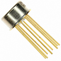
IC OPAMP GP 600KHZ LP TO99-8
Manufacturer
Analog Devices Inc
Datasheet
1.5962-8773802GA.pdf
(16 pages)
Specifications of 5962-8773802GA
Slew Rate
0.3 V/µs
Amplifier Type
General Purpose
Number Of Circuits
1
Gain Bandwidth Product
600kHz
Current - Input Bias
2.4nA
Voltage - Input Offset
25µV
Voltage - Supply, Single/dual (±)
±3 V ~ 18 V
Operating Temperature
-55°C ~ 125°C
Mounting Type
Through Hole
Package / Case
TO-99-8, Metal Can
Rail/rail I/o Type
No
Number Of Elements
1
Common Mode Rejection Ratio
120dB
Input Offset Voltage
0.025@±15VmV
Single Supply Voltage (typ)
Not RequiredV
Dual Supply Voltage (typ)
±5/±9/±12/±15V
Voltage Gain In Db
133.98dB
Power Supply Rejection Ratio
110.46dB
Power Supply Requirement
Dual
Shut Down Feature
No
Single Supply Voltage (min)
Not RequiredV
Single Supply Voltage (max)
Not RequiredV
Dual Supply Voltage (min)
±3V
Dual Supply Voltage (max)
±22V
Technology
Bipolar
Operating Temp Range
-55C to 125C
Operating Temperature Classification
Military
Mounting
Through Hole
Pin Count
8
Package Type
TO-99
Lead Free Status / RoHS Status
Lead free / RoHS Compliant
Current - Supply
-
Output Type
-
Current - Output / Channel
-
-3db Bandwidth
-
Lead Free Status / RoHS Status
Not Compliant, Lead free / RoHS Compliant
Other names
Q3964209
Available stocks
Company
Part Number
Manufacturer
Quantity
Price


ELECTRICAL SPECIFICATIONS
@ V
Table 1.
Parameter
INPUT OFFSET VOLTAGE
LONG-TERM STABILITY
INPUT OFFSET CURRENT
INPUT BIAS CURRENT
INPUT NOISE VOLTAGE
INPUT NOISE VOLTAGE DENSITY
INPUT NOISE CURRENT
INPUT NOISE CURRENT DENSITY
INPUT RESISTANCE
INPUT VOLTAGE RANGE
COMMON-MODE REJECTION RATIO
POWER SUPPLY REJECTION RATIO
LARGE-SIGNAL VOLTAGE GAIN
OUTPUT VOLTAGE SWING
SLEW RATE
CLOSED-LOOP BANDWIDTH
OPEN-LOOP OUTPUT RESISTANCE
POWER CONSUMPTION
OFFSET ADJUSTMENT RANGE
1
2
3
Long-term input offset voltage stability refers to the averaged trend line of V
hour of operation, changes in V
Sample tested.
Guaranteed by design.
Differential Mode
Common Mode
S
= ±15 V, T
2
A
= 25°C, unless otherwise noted.
3
1
2
2
OS
2
during the first 30 operating days are typically 2.5 μV.
Symbol
V
V
I
I
e
e
i
i
R
R
IVR
CMRR
PSRR
A
V
SR
BW
R
P
OS
B
np-p
n
np-p
n
OS
OS
IN
INCM
O
O
d
VO
/time
Conditions
0.1 Hz to 10 Hz
f
f
f
0.1 Hz to 10 Hz
f
f
f
V
V
R
V
R
R
R
R
A
V
V
Rp = 20 kn
O
O
O
O
O
O
L
L
L
L
L
CM
S
O
VCL
S
S
= 10 Hz
= 100 Hz
= 1000 Hz
= 10 Hz
= 100 Hz
= 1000 Hz
= ±3 V to ±18 V
≥ 2 kΩ
≥ 10 kΩ
≥ 2 kΩ
≥ 1 kΩ
≥ 2 kΩ
= ±15 V, no load
= ±3 V, no load
= ±10 V
= ±13 V
+ 1
Rev. E | Page 3 of 16
OS
2
2
vs. time over extended periods after the first 30 days of operation. Excluding the initial
Min
−0.2
26
±13
5000
±13.5
±12.5
±12.0
0.1
0.4
OP77E
Typ
10
0.3
0.3
+1.2
0.35
10.3
10.0
9.6
14
0.32
0.14
0.12
45
200
±14
0.1
0.7
12,000
±14.0
±13.0
±12.5
0.3
0.6
60
50
3.5
±3
Max
25
1.5
+2.0
0.6
18.0
13.0
11.0
30
0.80
0.23
0.17
1.0
3.0
60
4.5
Min
−0.2
18.5
±13
2000
±13.5
±12.5
±12.0
0.1
0.4
OP77F
Typ
20
0.4
0.3
+1.2
0.38
10.5
10.2
9.8
15
0.35
0.15
0.13
45
200
±14
0.1
0.7
6000
±14.0
±13.0
±12.5
0.3
0.6
60
50
3.5
±3
Max
60
2.8
+2.8
0.65
20.0
13.5
11.5
35
0.90
0.27
0.18
1.6
3.0
60
4.5
OP77
Unit
μV
μV/Mo
nA
nA
μV
nV/√Hz
pA
pA√Hz
MΩ
GΩ
V
μV/V
μV/V
V/mV
V
V/μs
MHz
Ω
mW
mV
p-p
p-p
Related parts for 5962-8773802GA
Image
Part Number
Description
Manufacturer
Datasheet
Request
R

Part Number:
Description:
OPTOCOUPLER HERMETIC 8-DIP
Manufacturer:
Avago Technologies US Inc.
Datasheet:

Part Number:
Description:
OPTOCOUPLER HERMETIC 8-DIP GW
Manufacturer:
Avago Technologies US Inc.
Datasheet:

Part Number:
Description:
Analog Multiplexer Single 8:1 16-Pin CDIP
Manufacturer:
Intersil
Datasheet:

Part Number:
Description:
ADC Single Semiflash 400KSPS 8-Bit Parallel 24-Pin CDIP
Manufacturer:
Maxim Integrated Products
Datasheet:
Part Number:
Description:
Analog Multiplexer Single 8:1 16-Pin CDIP
Manufacturer:
Maxim Integrated Products
Datasheet:
Part Number:
Description:
Analog Multiplexer Dual 8:1 28-Pin CDIP
Manufacturer:
Intersil
Datasheet:
Part Number:
Description:
CDIP 8/M�/Precision CMOS Analog Switch
Manufacturer:
Maxim Integrated Products

Part Number:
Description:
SPLD, PALCE16V8 Family, EECMOS Process, 300 Gates, 8 Macro Cells, 8 Reg., 8 User I/Os, 5V Supply, 15 Speed Grade, 20DIP
Manufacturer:
Cypress Semiconductor Corporation.
Datasheet:
Part Number:
Description:
OPTOCOUPLER MOSFET HERM 8DIP
Manufacturer:
Avago Technologies US Inc.
Datasheet:
Part Number:
Description:
OPTOCOUPLER GATE HERM SEAL 8DIP
Manufacturer:
Avago Technologies US Inc.
Datasheet:
Part Number:
Description:
OPTOCOUPLER GATE HERM SEAL 8DIP
Manufacturer:
Avago Technologies US Inc.
Datasheet:
Part Number:
Description:
OPTOCOUPLER GATE HERM SEAL 8DIP
Manufacturer:
Avago Technologies US Inc.
Datasheet:

Part Number:
Description:
ADC, LC2MOS High Speed 4-and 8-Channel 8-Bit ADCs
Manufacturer:
Analog Devices
Part Number:
Description:
ADC, LC2MOS High Speed 4-and 8-Channel 8-Bit ADCs
Manufacturer:
Analog Devices
Part Number:
Description:
OPTOCOUPLER HIGH CMR HERM 8DIP
Manufacturer:
Avago Technologies US Inc.
Datasheet: