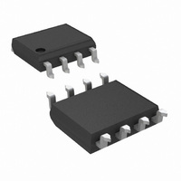
LMH6704MAX/NOPB National Semiconductor, LMH6704MAX/NOPB Datasheet - Page 3

LMH6704MAX/NOPB
Manufacturer Part Number
LMH6704MAX/NOPB
Description
IC BUFFER PROG GAIN 650MHZ 8SOIC
Manufacturer
National Semiconductor
Series
LMH®r
Datasheet
1.LMH6704MFNOPB.pdf
(12 pages)
Specifications of LMH6704MAX/NOPB
Amplifier Type
Buffer
Number Of Circuits
1
Slew Rate
3000 V/µs
-3db Bandwidth
650MHz
Current - Input Bias
5µA
Voltage - Input Offset
2000µV
Current - Supply
11.5mA
Current - Output / Channel
90mA
Voltage - Supply, Single/dual (±)
8 V ~ 12 V, ±4 V ~ 6 V
Operating Temperature
-40°C ~ 85°C
Mounting Type
Surface Mount
Package / Case
8-SOIC (3.9mm Width)
For Use With
LMH730227 - BOARD EVALUATION FOR SOIC PKGLMH730165 - BOARD EVALUATIONLMH730216 - BOARD EVAL HS MONO AMP SOT23
Lead Free Status / RoHS Status
Lead free / RoHS Compliant
Output Type
-
Gain Bandwidth Product
-
Other names
LMH6704MAX
CMIR
PSRR
V
I
I
R
R
R
C
Enable/Disable Performance (Disabled Low)
T
T
V
V
I
I
I
O
S
IH
IL
OZ
Symbol
ON
OFF
Electrical Characteristics
O
IH
IL
F
OUT
IN+
IN+
T
Note 1: Absolute Maximum Ratings indicate limits beyond which damage to the device may occur. Operating Ratings indicate conditions for which the device is
intended to be functional, but specific performance is not guaranteed. For guaranteed specifications, see the Electrical Characteristics tables.
Note 2: Electrical Table values apply only for factory testing conditions at the temperature indicated. Factory testing conditions result in very limited self-heating of
the device such that T
Min/Max ratings are based on production testing unless otherwise specified.
Note 3: The maximum output current (I
Note 4: Human Body Model, applicable std. MIL-STD-883, Method 3015.7. Machine Model, applicable std. JESD22-A115-A (ESD MM std. of JEDEC)
Field-Induced Charge-Device Model, applicable std. JESD22-C101-C (ESD FICDM std. of JEDEC).
Note 5: Slew Rate is the average of the rising and falling edges.
Note 6: Typical values represent the most likely parametric norm as determined at the time of characterization. Actual typical values may vary over time and will
also depend on the application and configuration. The typical values are not tested and are not guaranteed on shipped production material.
Note 7: Negative current implies current flowing out of the device.
Note 8: The maximum power dissipation is a function of T
P
D
A
& R
= (T
= +25˚C , A
G
J(MAX)
Common Mode Input Range
Power Supply Rejection Ratio
Output Voltage Swing
Linear Output Current
Supply Current (Enabled)
Supply Current (Disabled)
Internal R
Closed Loop Output Resistance
Input Resistance
Input Capacitance
Enable Time
Disable Time
Output Glitch
Enable Voltage
Disable Voltage
Disable Input Bias Current, High
Disable Input Bias Current, Low
Disabled Output Leakage
Current
– T
A
V
)/ θ
= +2, V
J
JA
= T
. All numbers apply for packages soldered directly onto a PC Board.
F
A
Parameter
and R
. No guarantee of parametric performance is indicated in the electrical tables under conditions of internal self-heating where T
S
=
G
±
5V, R
OUT
) is determined by device power dissipation limitations.
L
= 100Ω; unless specified.
(Note 2) (Continued)
V
DC
R
R
V
DIS = 2V, R
DIS = 0.8V, R
DC
DIS ≥ V
DIS ≤ V
DIS = V
DIS = 0V (Note 7)
A
IO
OUT
V
L
L
=
= 100Ω
= +1, V
≤ 15 mV
∞
≤ 80 mV
J(MAX)
IH
IL
+
, (Note 7)
, θ
OUT
L
Conditions
JA
=
L
. The maximum allowable power dissipation at any ambient temperature is
=
=
∞
3
±
∞
1.8V
(Note 6)
±
±
±
±
±
Min
±
375
2.0
3.18
3.12
48
47
1.9
3.3
3.2
0
55
(Note 6)
−100
±
±
11.5
0.25
0.05
Typ
±
465
0.2
±
52
10
10
50
−1
3.5
3.5
1
1
90
2
(Note 6)
0.925
−350
Max
12.5
13.7
563
±
±
±
0.9
0.8
50
25
50
www.national.com
Units
mV
J
mA
mA
MΩ
dB
pF
µA
µA
µA
ns
ns
>
Ω
Ω
V
V
V
PP
T
A
.


