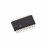
EL5373IUZ-T7 Intersil, EL5373IUZ-T7 Datasheet - Page 10

EL5373IUZ-T7
Manufacturer Part Number
EL5373IUZ-T7
Description
IC DRIVER TRIPLE 450MHZ 24-QSOP
Manufacturer
Intersil
Datasheet
1.EL5173ISZ-T7.pdf
(14 pages)
Specifications of EL5373IUZ-T7
Amplifier Type
Differential
Number Of Circuits
3
Output Type
Differential
Slew Rate
1100 V/µs
-3db Bandwidth
450MHz
Current - Input Bias
13µA
Voltage - Input Offset
3000µV
Current - Supply
12mA
Current - Output / Channel
50mA
Voltage - Supply, Single/dual (±)
4.75 V ~ 11 V, ±2.38 V ~ 5.5 V
Operating Temperature
-40°C ~ 85°C
Mounting Type
Surface Mount
Package / Case
24-QSOP
Lead Free Status / RoHS Status
Lead free / RoHS Compliant
Gain Bandwidth Product
-
Available stocks
Company
Part Number
Manufacturer
Quantity
Price
Company:
Part Number:
EL5373IUZ-T7
Manufacturer:
Intersil
Quantity:
1 000
Description of Operation and Application
Information
Product Description
The EL5173 and EL5373 are wide bandwidth, low power
and single/differential ended to differential output amplifiers.
They have a fixed gain of 2. The EL5173 is a single channel
differential amplifier. The EL5373 is a triple channel
differential amplifier. The EL5173 and EL5373 have a -3dB
bandwidth of 450MHz while driving a 200Ω differential load.
The EL5173 and EL5373 are available with a power-down
feature to reduce the power while the amplifiers are
disabled.
Input, Output and Supply Voltage Range
The EL5173 and EL5373 have been designed to operate
with a single supply voltage of 5V to 10V or split supplies
with its total voltage from 5V to 10V. The amplifiers have an
input common mode voltage range from -4.5V to 3.4V for
±5V supply. The differential mode input range (DMIR)
between the two inputs is from -2.3V to +2.3V. The input
voltage range at the REF pin is from -3.3V to 3.7V. If the
input common mode or differential mode signal is outside the
above-specified ranges, it will cause the output signal to
become distorted.
The output of the EL5173 and EL5373 can swing from -3.3V
to 3.6V at 200Ω differential load at ±5V supply. As the load
resistance becomes lower, the output swing is reduced.
Differential and Common Mode Gain Settings
As shown in the “Simplified Schematic” on page 9, since the
feedback resistors RF and the gain resistor are integrated with
200Ω and 400Ω, the EL5173 and EL5373 have a fixed gain of
2. The common mode gain is always one.
Driving Capacitive Loads and Cables
The EL5173 and EL5373 can drive 16pF differential
capacitor in parallel with 200Ω differential load with less than
3.5dB of peaking. If less peaking is desired in applications, a
small series resistor (usually between 5Ω to 50Ω) can be
placed in series with each output to eliminate most peaking.
However, this will reduce the gain slightly.
When used as a cable driver, double termination is always
recommended for reflection-free performance. For those
applications, a back-termination series resistor at the
amplifier’s output will isolate the amplifier from the cable and
allow extensive capacitive drive. However, other applications
may have high capacitive loads without a back-termination
resistor. Again, a small series resistor at the output can help
to reduce peaking.
Disable/Power-Down
The EL5173 and EL5373 can be disabled and placed their
outputs in a high impedance state. The turn-off time is about
1.2µs and the turn-on time is about 100ns. When disabled,
the amplifier’s supply current is reduced to 40µA for I
10
S
EL5173, EL5373
+ and
2.5µA for I
power consumption. The amplifier’s power-down can be
controlled by standard CMOS signal levels at the ENABLE
pin. The applied logic signal is relative to V
EN pin float or applying a signal that is less than 1.5V below
V
when the signal at EN pin is above V
Output Drive Capability
The EL5173 and EL5373 have internal short circuit
protection. Its typical short circuit current is ±55mA. If the
output is shorted indefinitely, the power dissipation could
easily increase such that the part will be destroyed.
Maximum reliability is maintained if the output current never
exceeds ±60mA. This limit is set by the design of the internal
metal interconnect.
Power Dissipation
With the high output drive capability of the EL5173 and
EL5373, it is possible to exceed the +125°C absolute
maximum junction temperature under certain load current
conditions. Therefore, it is important to calculate the maximum
junction temperature for the application to determine if the
load conditions or package types need to be modified for the
amplifier to remain in the safe operating area.
The maximum power dissipation allowed in a package is
determined according to Equation 1:
Where:
• T
• T
• θ
The maximum power dissipation actually produced by an IC
is the total quiescent supply current times the total power
supply voltage, plus the power in the IC due to the load, or
as expressed in Equation 2:
PD
Where:
• V
• I
• ΔV
• R
• I
• i = Number of channels
PD
S
application
+ will enable the amplifier. The amplifier will be disabled
SMAX
LOAD
MAX
JA
AMAX
JMAX
S
LD
=
O
= Total supply voltage
i
= Thermal resistance of the package
×
= Differential load resistance
= Maximum differential output voltage of the
=
⎛
⎜
⎝
= Load current
= Maximum quiescent supply current per channel
V
= Maximum junction temperature
= Maximum ambient temperature
S
T
-------------------------------------------- -
S
- typically, thereby effectively eliminating the
JMAX
×
I
SMAX
Θ
–
JA
T
AMAX
+
V
S
×
ΔV
----------- -
R
LD
O
⎞
⎟
⎠
S
+ - 0.5V.
S
+ pin. Letting the
September 14, 2010
(EQ. 2)
FN7312.8
(EQ. 1)


