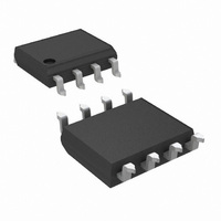
LMH6619MA/NOPB National Semiconductor, LMH6619MA/NOPB Datasheet - Page 19

LMH6619MA/NOPB
Manufacturer Part Number
LMH6619MA/NOPB
Description
IC AMP DUAL RRIO 130MHZ 8-SOIC
Manufacturer
National Semiconductor
Series
PowerWise®r
Specifications of LMH6619MA/NOPB
Amplifier Type
Voltage Feedback
Number Of Circuits
2
Output Type
Rail-to-Rail
Slew Rate
57 V/µs
Gain Bandwidth Product
58MHz
-3db Bandwidth
140MHz
Current - Input Bias
1.5µA
Voltage - Input Offset
100µV
Current - Supply
1.45mA
Current - Output / Channel
35mA
Voltage - Supply, Single/dual (±)
2.7 V ~ 11 V, ±1.35 V ~ 5.5 V
Operating Temperature
-40°C ~ 125°C
Mounting Type
Surface Mount
Package / Case
8-SOIC (3.9mm Width)
Bandwidth
130 MHz
Common Mode Rejection Ratio
96
Current, Input Bias
1 μA (NPN Active), -1.5 μA (PNP Active)
Current, Input Offset
0.01 μA
Current, Output
±35 mA
Current, Supply
1.3 mA
Impedance, Thermal
160 °C/W
Number Of Amplifiers
Dual
Package Type
SOIC-8
Resistance, Input
8 Megohms
Temperature, Operating, Range
-40 to +125 °C
Time, Fall
30 ns
Time, Rise
30 ns
Voltage, Gain
100 dB
Voltage, Input
2.7 to 11 V
Voltage, Noise
10 nV/sqrt Hz
Voltage, Offset
0.1 mV
Voltage, Output, High
230 mV
Voltage, Output, Low
255 mV
Voltage, Supply
5 V
Number Of Channels
2
Voltage Gain Db
100 dB
Common Mode Rejection Ratio (min)
81 dB
Input Offset Voltage
0.6 mV at 5 V
Operating Supply Voltage
3 V, 5 V, 9 V
Supply Current
3 mA at 5 V
Maximum Operating Temperature
+ 125 C
Minimum Operating Temperature
- 40 C
For Use With
551600075-001 - BOARD FOR SOIC LMH6612/19551600074-001 - BOARD FOR SOIC LMH6612/19
Lead Free Status / RoHS Status
Lead free / RoHS Compliant
Other names
LMH6619MA
Application Information
The LMH6618 and LMH6619 are based on National
Semiconductor’s proprietary VIP10 dielectrically isolated
bipolar process. This device family architecture features the
following:
•
•
•
•
With 3V supplies and a common mode input voltage range
that extends beyond either supply rail, the LMH6618 and
LMH6619 are well suited to many low voltage/low power ap-
plications. Even with 3V supplies, the −3 dB BW
(at A
The LMH6618 and LMH6619 are designed to avoid output
phase reversal. With input over-drive, the output is kept near
the supply rail (or as close to it as mandated by the closed
loop gain setting and the input voltage). Figure 1 shows the
input and output voltage when the input voltage significantly
exceeds the supply voltages.
FIGURE 1. Input and Output Shown with CMVR Exceeded
If the input voltage range is exceeded by more than a diode
drop beyond either rail, the internal ESD protection diodes will
start to conduct. The current flow in these ESD diodes should
be externally limited.
The LMH6618 can be shutdown by connecting the
DISABLE pin to a voltage 0.5V below the supply midpoint
which will reduce the supply current to typically less than
Complimentary bipolar devices with exceptionally high f
(
bias current.
Common emitter push-push output stage. This
architecture allows the output to reach within millivolts of
either supply rail.
Consistent performance from any supply voltage
11V)
important specifications (e.g. BW, SR, I
Significant power saving compared to competitive devices
on the market with similar performance.
∼
V
8 GHz) even under low supply voltage (2.7V) and low
= +1) is typically 120 MHz.
with little variation with supply voltage for the most
OUT
.)
20195825
(2.7V -
t
19
100 µA. The DISABLE pin is “active low” and should be con-
nected through a resistor to V
down is guaranteed when the DISABLE pin is 0.5V below the
supply midpoint at any operating supply voltage and temper-
ature.
In the shutdown mode, essentially all internal device biasing
is turned off in order to minimize supply current flow and the
output goes into high impedance mode. During shutdown, the
input stage has an equivalent circuit as shown in Figure 2.
When the LMH6618 is shutdown, there may be current flow
through the internal diodes shown, caused by input potential,
if present. This current may flow through the external feed-
back resistor and result in an apparent output signal. In most
shutdown applications the presence of this output is incon-
sequential. However, if the output is “forced” by another de-
vice, the other device will need to conduct the current
described in order to maintain the output potential.
To keep the output at or near ground during shutdown when
there is no other device to hold the output low, a switch using
a transistor can be used to shunt the output to ground.
SINGLE CHANNEL ADC DRIVER
The low noise and wide bandwidth make the LMH6618 an
excellent choice for driving a 12-bit ADC. Figure 3 shows the
schematic of the LMH6618 driving an ADC121S101. The AD-
C121S101 is a single channel 12-bit ADC. The LMH6618 is
set up in a 2nd order multiple-feedback configuration with a
gain of −1. The −3 dB point is at 500 kHz and the −0.01 dB
point is at 100 kHz. The 22Ω resistor and 390 pF capacitor
form an antialiasing filter for the ADC121S101. The capacitor
also stores and delivers charge to the switched capacitor in-
put of the ADC. The capacitive load on the LMH6618 created
by the 390 pF capacitor is decreased by the 22Ω resistor.
Table 1 shows the performance data of the LMH6618 and the
ADC121S101.
FIGURE 2. Input Equivalent Circuit During Shutdown
+
for normal operation. Shut-
www.national.com
20195839


