LM324ADG ON Semiconductor, LM324ADG Datasheet - Page 2
LM324ADG
Manufacturer Part Number
LM324ADG
Description
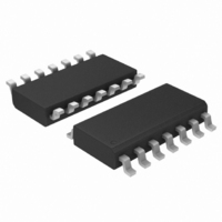
IC OPAMP QUAD SGL 32VDC 14-SOIC
Manufacturer
ON Semiconductor
Datasheet
1.LM324DR2G.pdf
(15 pages)
Specifications of LM324ADG
Amplifier Type
General Purpose
Number Of Circuits
4
Slew Rate
0.6 V/µs
Gain Bandwidth Product
1MHz
Current - Input Bias
45nA
Voltage - Input Offset
2000µV
Current - Supply
1.4mA
Current - Output / Channel
40mA
Voltage - Supply, Single/dual (±)
3 V ~ 32 V, ±1.5 V ~ 16 V
Operating Temperature
0°C ~ 70°C
Mounting Type
Surface Mount
Package / Case
14-SOIC (3.9mm Width), 14-SOL
Number Of Channels
4
Common Mode Rejection Ratio (min)
65 dB
Input Voltage Range (max)
Positive Rail - 1.7 V
Input Voltage Range (min)
Negative Rail
Input Offset Voltage
3 mV
Input Bias Current (max)
100 nA
Output Current (typ)
40 mA
Operating Supply Voltage
32 V
Supply Current
1.2 mA
Maximum Operating Temperature
+ 70 C
Minimum Operating Temperature
0 C
Dual Supply Voltage
+/- 3 V, +/- 5 V, +/- 9 V
Maximum Dual Supply Voltage
+/- 16 V
Minimum Dual Supply Voltage
+/- 1.5 V
Mounting Style
SMD/SMT
Shutdown
No
Supply Voltage (max)
32 V
Supply Voltage (min)
3 V
Technology
Bipolar
Voltage Gain Db
100 dB
Lead Free Status / RoHS Status
Lead free / RoHS Compliant
Output Type
-
-3db Bandwidth
-
Lead Free Status / Rohs Status
Lead free / RoHS Compliant
Other names
LM324ADG
LM324ADGOS
LM324ADGOS
Available stocks
Company
Part Number
Manufacturer
Quantity
Price

Part Number:
LM324ADG
Manufacturer:
ON/安森美
Quantity:
20 000


Stresses exceeding Maximum Ratings may damage the device. Maximum Ratings are stress ratings only. Functional operation above the
Recommended Operating Conditions is not implied. Extended exposure to stresses above the Recommended Operating Conditions may affect
device reliability.
1. Split Power Supplies.
2. For supply voltages less than 32 V, the absolute maximum input voltage is equal to the supply voltage.
3. All R
4. NCV2902 is qualified for automitive use.
MAXIMUM RATINGS
Power Supply Voltages
Input Differential Voltage Range (Note 1)
Input Common Mode Voltage Range (Note 2)
Output Short Circuit Duration
Junction Temperature
Thermal Resistance, Junction−to−Air (Note 3)
Storage Temperature Range
ESD Protection at any Pin
Operating Ambient Temperature Range
qJA
Single Supply
Split Supplies
Human Body Model
Machine Model
measurements made on evaluation board with 1 oz. copper traces of minimum pad size. All device outputs were active.
(T
A
= + 25°C, unless otherwise noted.)
Rating
LM2902V, NCV2902 (Note 4)
http://onsemi.com
LM324, 324A
Case 948G
Case 751A
Case 646
LM2902
2
LM224
V
Symbol
CC
R
V
V
V
V
T
t
T
T
SC
IDR
ICR
qJA
esd
CC
, V
stg
A
J
EE
−65 to +150
−40 to +105
−40 to +125
Continuous
−25 to +85
−0.3 to 32
0 to +70
Value
2000
±16
±32
150
118
156
190
200
32
°C/W
Unit
Vdc
Vdc
Vdc
°C
°C
°C
V
Related parts for LM324ADG
Image
Part Number
Description
Manufacturer
Datasheet
Request
R

Part Number:
Description:
LM324
Manufacturer:
ON Semiconductor
Datasheet:
Part Number:
Description:
Single Supply Quad Operational Amplifiers
Manufacturer:
On Semiconductor
Part Number:
Description:
Single Supply Quad Operational Amplifier
Manufacturer:
ON Semiconductor
Datasheet:
Part Number:
Description:
ON Semiconductor [VOLTAGE REGULATOR]
Manufacturer:
ON Semiconductor
Datasheet:
Part Number:
Description:
357-036-542-201 CARDEDGE 36POS DL .156 BLK LOPRO
Manufacturer:
ON Semiconductor
Datasheet:
Part Number:
Description:
357-036-542-201 CARDEDGE 36POS DL .156 BLK LOPRO
Manufacturer:
ON Semiconductor
Datasheet:
Part Number:
Description:
357-036-542-201 CARDEDGE 36POS DL .156 BLK LOPRO
Manufacturer:
ON Semiconductor
Datasheet:
Part Number:
Description:
357-036-542-201 CARDEDGE 36POS DL .156 BLK LOPRO
Manufacturer:
ON Semiconductor
Datasheet:
Part Number:
Description:
357-036-542-201 CARDEDGE 36POS DL .156 BLK LOPRO
Manufacturer:
ON Semiconductor
Datasheet:
Part Number:
Description:
357-036-542-201 CARDEDGE 36POS DL .156 BLK LOPRO
Manufacturer:
ON Semiconductor
Datasheet:
Part Number:
Description:
357-036-542-201 CARDEDGE 36POS DL .156 BLK LOPRO
Manufacturer:
ON Semiconductor
Datasheet:
Part Number:
Description:
357-036-542-201 CARDEDGE 36POS DL .156 BLK LOPRO
Manufacturer:
ON Semiconductor
Datasheet:
Part Number:
Description:
357-036-542-201 CARDEDGE 36POS DL .156 BLK LOPRO
Manufacturer:
ON Semiconductor
Datasheet:
Part Number:
Description:
357-036-542-201 CARDEDGE 36POS DL .156 BLK LOPRO
Manufacturer:
ON Semiconductor
Datasheet: