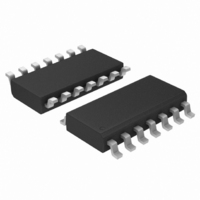
LM324ADG ON Semiconductor, LM324ADG Datasheet - Page 8

LM324ADG
Manufacturer Part Number
LM324ADG
Description
IC OPAMP QUAD SGL 32VDC 14-SOIC
Manufacturer
ON Semiconductor
Datasheet
1.LM324DR2G.pdf
(15 pages)
Specifications of LM324ADG
Amplifier Type
General Purpose
Number Of Circuits
4
Slew Rate
0.6 V/µs
Gain Bandwidth Product
1MHz
Current - Input Bias
45nA
Voltage - Input Offset
2000µV
Current - Supply
1.4mA
Current - Output / Channel
40mA
Voltage - Supply, Single/dual (±)
3 V ~ 32 V, ±1.5 V ~ 16 V
Operating Temperature
0°C ~ 70°C
Mounting Type
Surface Mount
Package / Case
14-SOIC (3.9mm Width), 14-SOL
Number Of Channels
4
Common Mode Rejection Ratio (min)
65 dB
Input Voltage Range (max)
Positive Rail - 1.7 V
Input Voltage Range (min)
Negative Rail
Input Offset Voltage
3 mV
Input Bias Current (max)
100 nA
Output Current (typ)
40 mA
Operating Supply Voltage
32 V
Supply Current
1.2 mA
Maximum Operating Temperature
+ 70 C
Minimum Operating Temperature
0 C
Dual Supply Voltage
+/- 3 V, +/- 5 V, +/- 9 V
Maximum Dual Supply Voltage
+/- 16 V
Minimum Dual Supply Voltage
+/- 1.5 V
Mounting Style
SMD/SMT
Shutdown
No
Supply Voltage (max)
32 V
Supply Voltage (min)
3 V
Technology
Bipolar
Voltage Gain Db
100 dB
Lead Free Status / RoHS Status
Lead free / RoHS Compliant
Output Type
-
-3db Bandwidth
-
Lead Free Status / Rohs Status
Lead free / RoHS Compliant
Other names
LM324ADG
LM324ADGOS
LM324ADGOS
Available stocks
Company
Part Number
Manufacturer
Quantity
Price
Part Number:
LM324ADG
Manufacturer:
ON/安森美
Quantity:
20 000
Figure 13. High Impedance Differential Amplifier
e
e
V
1
2
in
MC1403
V
R1
CC
C1
-
+
LM324
-
LM324
+
1/4
1/4
Figure 11. Voltage Reference
a R1
b R1
e
o
= C (1 + a + b) (e
R2
R2
2.5 V
V
ref
C R
C R
1
1
R2
-
+
LM324
V
1/4
O
R1
LM324
-
+
2
1/4
= 2.5 V
- e
V
R
C
CC
1
R
)
+
-
LM324
1 +
1/4
R
R1
R2
R1
V
R
O
Bandpass
Figure 15. Bi−Quad Filter
Output
http://onsemi.com
Vref
e
o
-
+
LM324
1/4
C
8
V
ref
R
V
V
V
ref
-
+
LM324
in
ref
1/4
=
R3
Where: T
Where:
V
1
2
ref
100 k
V
R1
CC
Figure 14. Comparator with Hysteresis
V
V
inH
inL
T
Figure 12. Wien Bridge Oscillator
H =
BP
N
=
V
=
10 k
ref
= Passband Notch Gain
= Center Frequency Gain
R1 + R2
R1 + R2
R1 + R2
+
-
LM324
R
-
+
R1
1/4
R1
LM324
100 k
R1
R2
1/4
C1
5.0 k
(V
(V
(V
OL
OH
OH
-
+
C
LM324
50 k
1/4
- V
- V
- V
For: f
For:
For:
For:
R
ref
V
ref
OL
V
Notch Output
O
) + V
CC
) + V
)
f
R1 = QR
R2 =
R3 = T
C1 = 10C
Q = 10
T
T
o
V
C
V
o
BP
N
V
OH
= 2 p RC
OL
ref
ref
= 1.0 kHz
O
= 1
= 1
T
R1
N R2
BP
1
For: f
f
o
=
V
R = 160 kW
C = 0.001 mF
R1 = 1.6 MW
R2 = 1.6 MW
R3 = 1.6 MW
O
2 p RC
V
R = 16 kW
C = 0.01 mF
V
o
Hysteresis
ref
inL
1
= 1.0 kHz
V
=
ref
1
2
V
inH
V
CC


