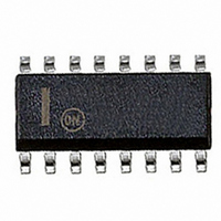
NE5517D ON Semiconductor, NE5517D Datasheet - Page 3

NE5517D
Manufacturer Part Number
NE5517D
Description
IC AMP XCONDUCTANCE DUAL 16-SOIC
Manufacturer
ON Semiconductor
Datasheet
1.NE5517DG.pdf
(14 pages)
Specifications of NE5517D
Amplifier Type
Transconductance
Number Of Circuits
2
Output Type
Push-Pull
Slew Rate
50 V/µs
Gain Bandwidth Product
2MHz
Current - Input Bias
400nA
Voltage - Input Offset
400µV
Current - Supply
2.6mA
Current - Output / Channel
650µA
Voltage - Supply, Single/dual (±)
4 V ~ 44 V, ±2 V ~ 22 V
Operating Temperature
0°C ~ 70°C
Mounting Type
Surface Mount
Package / Case
16-SOIC (3.9mm Width)
Number Of Channels
2
Input Offset Voltage
5 mV
Supply Voltage (max)
44 V
Supply Current
4 mA
Maximum Operating Temperature
+ 70 C
Minimum Operating Temperature
0 C
Common Mode Rejection Ratio (min)
80 dB
Input Voltage Range (max)
Positive Rail - 3 V
Maximum Power Dissipation
1125 mW
Mounting Style
SMD/SMT
Lead Free Status / RoHS Status
Contains lead / RoHS non-compliant
-3db Bandwidth
-
Lead Free Status / Rohs Status
Details
Available stocks
Company
Part Number
Manufacturer
Quantity
Price
Part Number:
NE5517D
Manufacturer:
NXP/恩智浦
Quantity:
20 000
MAXIMUM RATINGS
Stresses exceeding Maximum Ratings may damage the device. Maximum Ratings are stress ratings only. Functional operation above the
Recommended Operating Conditions is not implied. Extended exposure to stresses above the Recommended Operating Conditions may affect
device reliability.
1. For selections to a supply voltage above ±22 V, contact factory.
2. The following derating factors should be applied above 25 °C
3. Buffer output current should be limited so as to not exceed package dissipation.
Supply Voltage (Note 1)
Power Dissipation, T
Thermal Resistance, Junction−to−Ambient
Differential Input Voltage
Diode Bias Current
Amplifier Bias Current
Output Short-Circuit Duration
Buffer Output Current (Note 3)
Operating Temperature Range
Operating Junction Temperature
DC Input Voltage
Storage Temperature Range
Lead Soldering Temperature (10 sec max)
NE5517N, NE5517AN
NE5517D, AU5517D
D Package
N Package
NE5517N, NE5517AN
AU5517T
N package at 10.6 mW/°C
D package at 7.1 mW/°C.
amb
= 25 °C (Still Air) (Note 2)
NOTE:
INPUT
16
INPUT
1
BIAS
BIAS
AMP
AMP
B
A
V+ of output buffers and amplifiers are internally connected.
Rating
DIODE
DIODE
15
2
BIAS
BIAS
B
A
NE5517, NE5517A, AU5517
INPUT
14
INPUT
3
(+)
(+)
B
A
Figure 2. Connection Diagram
http://onsemi.com
−
+
+
−
13
INPUT
INPUT
4
(−)
(−)
B
A
B
A
3
OUTPUT
OUTPUT
12
5
B
A
11
V+ (1)
6
V−
Symbol
R
I
I
T
V
T
T
V
ABC
I
OUT
V
P
amb
T
I
SC
qJA
DC
stg
sld
BUFFER
BUFFER
D
IN
S
D
J
INPUT
10
INPUT
7
B
A
OUTPUT
OUTPUT
BUFFER
BUFFER
9
8
−40 °C to +125 °C
−65 °C to +150 °C
B
A
44 V
0 °C to +70 °C
+V
Indefinite
Value
S
DC
1500
1125
±5.0
140
150
230
2.0
2.0
94
20
to −V
or ±22
S
°C/W
Unit
mW
mA
mA
mA
°C
°C
°C
°C
V
V


