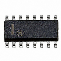
NE5517D ON Semiconductor, NE5517D Datasheet - Page 8

NE5517D
Manufacturer Part Number
NE5517D
Description
IC AMP XCONDUCTANCE DUAL 16-SOIC
Manufacturer
ON Semiconductor
Datasheet
1.NE5517DG.pdf
(14 pages)
Specifications of NE5517D
Amplifier Type
Transconductance
Number Of Circuits
2
Output Type
Push-Pull
Slew Rate
50 V/µs
Gain Bandwidth Product
2MHz
Current - Input Bias
400nA
Voltage - Input Offset
400µV
Current - Supply
2.6mA
Current - Output / Channel
650µA
Voltage - Supply, Single/dual (±)
4 V ~ 44 V, ±2 V ~ 22 V
Operating Temperature
0°C ~ 70°C
Mounting Type
Surface Mount
Package / Case
16-SOIC (3.9mm Width)
Number Of Channels
2
Input Offset Voltage
5 mV
Supply Voltage (max)
44 V
Supply Current
4 mA
Maximum Operating Temperature
+ 70 C
Minimum Operating Temperature
0 C
Common Mode Rejection Ratio (min)
80 dB
Input Voltage Range (max)
Positive Rail - 3 V
Maximum Power Dissipation
1125 mW
Mounting Style
SMD/SMT
Lead Free Status / RoHS Status
Contains lead / RoHS non-compliant
-3db Bandwidth
-
Lead Free Status / Rohs Status
Details
Available stocks
Company
Part Number
Manufacturer
Quantity
Price
Part Number:
NE5517D
Manufacturer:
NXP/恩智浦
Quantity:
20 000
Linearizing Diodes
invalid and the transconductance increases non-linearly.
Figure 22 shows how the internal diodes can linearize the
transfer function of the operational amplifier. Assume D
and D
current is I
that is: I
geometries and are subject to similar voltages and
temperatures, the following equation is true:
The only limitation is that the signal current should not
exceed I
For V
For the diodes and the input transistors that have identical
3
I
S
are biased with current sources and the input signal
IN
4
D
= (I
.
I
greater than a few millivolts, Equation 3 becomes
S
T
q In
S
B
I D
. Since I
2
1/2I
Figure 22. Linearizing Diode
D
− I
* I
3
D
I D
I
I
0
2
D
2
O
), I
S
1/2I
) I
* I
+ I
D
5
I D
+VS
2
S
S
= (I
I
S
D
4
+ KT q In
) I
2
I
+ I
I
D
B
B
S
V
+ I
for |I
IN
5
D
2
0
= I
)
Q
S
1 2(I
1 2(I
R
4
| t
I 0 + I 5 * I 4
4
B
= R
I
4
R
and I
2
I
B
B
2
2
D
/ /R
−VS
) I
* I
I
B
3
NE5517, NE5517A, AU5517
O
O
I
5
5
)
)
R
I 0 + 2 I
3
4
3
− I
I
5
+
−
4
NE5517
http://onsemi.com
(eq. 6)
+V
S
= I
CC
11
6
I
I
B
D
TYPICAL VALUES: R
0
R
Figure 23.
2
,
1
1
V
8
C
I
OUT
I
ABC
Impedance Buffer
maximum value of I
which the amplifier will function therefore determines the
overall dynamic range. At low values of I
very low input bias current is desired. A Darlington
amplifier with constant-current source (Q
D
Voltage-Controlled Amplifier
input-voltage into small values (mV range) so the amplifier
operates in a linear manner.
It is:
Since g
is controlled by the voltage V
is valid:
the current mirrors. This circuit is the base for many
applications of the AU5517/NE5517.
5
8
The upper limit of transconductance is defined by the
In Figure 23, the voltage divider R
When V
The 1.2 V is the voltage across two base-emitter baths in
, and R
R
R
R
R
R
R
L
1
2
3
4
L
S
7
M
= 47kW
= 10kW
= 200W
= 200W
= 100kW
= 47kW
is directly proportional to I
1
C
) suits the need.
is taken relative to −V
A +
I
(g
OUT
M
+ *V
V
in mmhos for I
I
V
APPLICATIONS
B
ABC
R
V
OUT
S
(3) g
IN
(2.0 mA). The lowest value of I
OUT
8
+
+
+V
INT
INT
−V
IN
V
+ I
M
CC
OUT
(V
R
CC
@
= 19.2 I
2
C
R
C
OUT
R
) R
* 1.2V)
2
in a simple way.
R
3
R
) R
ABC
1
@ R
CC
3
3
ABC
@ g
ABC
L
3
in mA)
the following formula
;
@ g
M
2
, the amplification
@ R
, R
M
14
B
;
, Q
, a buffer with
L
3
15
divides the
, Q
16
B
, D
for
7
,


