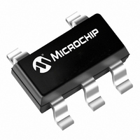
MCP1321T-29LE/OT Microchip Technology, MCP1321T-29LE/OT Datasheet - Page 8

MCP1321T-29LE/OT
Manufacturer Part Number
MCP1321T-29LE/OT
Description
IC SUPERVISOR 2.9V OD/PP SOT23-5
Manufacturer
Microchip Technology
Type
Simple Reset/Power-On Resetr
Specifications of MCP1321T-29LE/OT
Number Of Voltages Monitored
1
Package / Case
SOT-23-5, SC-74A, SOT-25
Output
Open Drain, Push-Pull
Reset
Active High/Active Low
Reset Timeout
140 ms Minimum
Voltage - Threshold
2.9V
Operating Temperature
-40°C ~ 125°C
Mounting Type
Surface Mount
Chip Enable Signals
No
Minimum Operating Temperature
- 40 C
Output Type
Active High or Active Low or Open Drain or Push-Pull
Power Fail Detection
No
Monitored Voltage
2 V to 4.7 V
Undervoltage Threshold
2.857 V
Overvoltage Threshold
2.944 V
Manual Reset
Resettable
Watchdog
Yes
Battery Backup Switching
No
Power-up Reset Delay (typ)
2240 ms
Supply Voltage (max)
5.5 V
Supply Voltage (min)
1 V
Supply Current (typ)
10 uA
Maximum Power Dissipation
240 mW
Mounting Style
SMD/SMT
Maximum Operating Temperature
+ 125 C
Input Voltage
5.5V
No. Of Outputs
1
Power Dissipation Pd
240mW
Supply Voltage Range
1V To 5.5V
No. Of Pins
5
Operating Temperature Range
-40°C To +125°C
Filter Terminals
SMD
Supply Voltage Min
1V
Rohs Compliant
Yes
Lead Free Status / RoHS Status
Lead free / RoHS Compliant
Lead Free Status / RoHS Status
Lead free / RoHS Compliant, Lead free / RoHS Compliant
Other names
MCP1321T-29LE/OT
MCP1321T-29LE/OTTR
MCP1321T-29LE/OTTR
Available stocks
Company
Part Number
Manufacturer
Quantity
Price
Company:
Part Number:
MCP1321T-29LE/OT
Manufacturer:
MICROCHIP
Quantity:
12 000
MCP131X/2X
FIGURE 1-1:
TABLE 1-1:
DS21985B-page 8
Electrical Specifications: Unless otherwise indicated, all limits are specified for V
(only MCP1320, MCP1321, and MCP1322), T
Falling V
to RST or RST Active
V
Reset active time
(MR Rising Edge, POR/BOR
Inactive, or WDT time out) to RST/
RST Inactive
RST Rise Time after RST Active
(Push-Pull Outputs only)
RST Rise Time after RST Inactive
(Push-Pull Outputs only)
RST Fall Time after RST Inactive
RST Fall Time after RST Active
Note 1:
DD
V
RST
RST
Rise Rate
DD
2:
3:
t
RR
V
unknown while V
DD
DD
These parameters are for design guidance only and are not 100% tested.
Custom ordered Reset active time; minimum order volume requirement.
Designed to be independent of V
0.1 V/s (@ +25°C).
Parameters
V
Trip Point Detected
1V
< 1V is outside the device operating specification. The RST (or RST) output state is
TRIPMIN
V
DEVICE VOLTAGE AND RESET PIN TIMINGS
TRIPMAX
V
Device Voltage and Reset Pin Waveforms.
TRIP
DD
V
< 1V.
TRIPAC
+ V
t
RST
Sym
t
t
RPD
t
RST
t
t
RR
RT
FT
HYS
DD
A
rise rate. Device characterization was done with a rise rate as slow as
= -40°C to +125°C.
1120
Min
140
1.0
20
—
—
—
—
—
Note 3
1600
Typ
650
200
1.4
30
5
5
5
5
2240
Max
280
2.0
40
—
—
—
—
—
Units
t
ms
ms
ms
ms
RPD
µs
µs
µs
µs
µs
DD
= 1V to 5.5V, R
V
V
V
V
C
Note 2
Note 2
Standard Time Out
Note 2
For RST 10% to 90% of V
C
For RST 10% to 90% of V
C
For RST 90% to 10% of V
C
For RST 90% to 10% of V
C
© 2007 Microchip Technology Inc.
DD
TRIPMAX
TRIPMIN
DD
L
L
L
L
L
= 50 pF (Note 1)
= 50 pF (Note 1)
= 50 pF (Note 1)
= 50 pF (Note 1)
= 50 pF (Note 1)
ramped from
falling @ 5 mV/µs,
Conditions
– 200 mV,
+ 250 mV down to
PU
= 100 kΩ
t
RST
DD
DD
DD
DD
,
,
,
,


