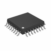
ADM1069ASTZ Analog Devices Inc, ADM1069ASTZ Datasheet - Page 26

ADM1069ASTZ
Manufacturer Part Number
ADM1069ASTZ
Description
IC SUPERVISOR/SEQUENCER 32-LQFP
Manufacturer
Analog Devices Inc
Type
Sequencerr
Datasheet
1.EVAL-ADM1069LQEBZ.pdf
(32 pages)
Specifications of ADM1069ASTZ
Number Of Voltages Monitored
8
Output
Programmable
Voltage - Threshold
8 Selectable Threshold Combinations
Operating Temperature
-40°C ~ 85°C
Mounting Type
Surface Mount
Package / Case
32-LQFP
For Use With
EVAL-ADM1069LQEBZ - BOARD EVALUATION FOR ADM1069LQ
Lead Free Status / RoHS Status
Lead free / RoHS Compliant
Reset
-
Reset Timeout
-
Available stocks
Company
Part Number
Manufacturer
Quantity
Price
Company:
Part Number:
ADM1069ASTZ
Manufacturer:
AKM
Quantity:
940
Company:
Part Number:
ADM1069ASTZ
Manufacturer:
AD
Quantity:
885
Company:
Part Number:
ADM1069ASTZ
Manufacturer:
Analog Devices Inc
Quantity:
10 000
Part Number:
ADM1069ASTZ
Manufacturer:
ADI/亚德诺
Quantity:
20 000
Company:
Part Number:
ADM1069ASTZ-REEL
Manufacturer:
Analog Devices Inc
Quantity:
10 000
Part Number:
ADM1069ASTZ-REEL
Manufacturer:
ADI/亚德诺
Quantity:
20 000
Company:
Part Number:
ADM1069ASTZ-REEL7
Manufacturer:
Analog Devices Inc
Quantity:
10 000
ADM1069
The device also has several identification registers (read-only)
that can be read across the SMBus. Table 12 lists these registers
with their values and functions.
Table 12. Identification Register Values and Functions
Name
MANID
REVID
MARK1
MARK2
General SMBus Timing
Figure 36, Figure 37, and Figure 38 are timing diagrams for
general read and write operations using the SMBus. The SMBus
specification defines specific conditions for different types of
read and write operations, which are discussed in the Write
Operations and Read Operations sections.
The general SMBus protocol operates as follows:
Step 1
The master initiates data transfer by establishing a start condition,
defined as a high-to-low transition on the serial data line SDA,
while the serial clock line SCL remains high. This indicates that
a data stream follows. All slave peripherals connected to the serial
bus respond to the start condition and shift in the next eight bits,
consisting of a 7-bit slave address (MSB first) plus an R/ W bit.
This bit determines the direction of the data transfer, that is,
whether data is written to or read from the slave device (0 = write,
1 = read).
The peripheral whose address corresponds to the transmitted
address responds by pulling the data line low during the low period
before the ninth clock pulse, known as the acknowledge bit, and
by holding it low during the high period of this clock pulse.
Address
0xF4
0xF5
0xF6
0xF7
(CONTINUED)
(CONTINUED)
SDA
SCL
START BY
SDA
SCL
MASTER
Value
0x41
0x02
0x00
0x00
1
1
Manufacturer ID for Analog Devices
Silicon revision
Software brand
Software brand
Function
1
D7
0
D6
SLAVE ADDRESS
0
FRAME 1
D5
1
D4
1
DATA BYTE
FRAME 3
A1
D3
Figure 36. General SMBus Write Timing Diagram
A0
D2
R/W
ACK. BY
D1
SLAVE
Rev. B | Page 26 of 32
9
D0
ACK. BY
SLAVE
1
9
D7
D6
1
All other devices on the bus remain idle while the selected device
waits for data to be read from or written to it. If the R/ W bit is a 0,
the master writes to the slave device. If the R/ W bit is a 1, the
master reads from the slave device.
Step 2
Data is sent over the serial bus in sequences of nine clock pulses:
eight bits of data followed by an acknowledge bit from the slave
device. Data transitions on the data line must occur during the
low period of the clock signal and remain stable during the high
period because a low-to-high transition when the clock is high
could be interpreted as a stop signal. If the operation is a write
operation, the first data byte after the slave address is a command
byte. This command byte tells the slave device what to expect next.
It may be an instruction telling the slave device to expect a block
write, or it may be a register address that tells the slave where
subsequent data is to be written. Because data can flow in only
one direction, as defined by the R/ W bit, sending a command
to a slave device during a read operation is not possible. Before
a read operation, it may be necessary to perform a write operation
to tell the slave what sort of read operation to expect and/or the
address from which data is to be read.
Step 3
When all data bytes have been read or written, stop conditions
are established. In write mode, the master pulls the data line high
during the 10th clock pulse to assert a stop condition. In read
mode, the master device releases the SDA line during the low
period before the ninth clock pulse, but the slave device does not
pull it low. This is known as a no acknowledge. The master then
takes the data line low during the low period before the 10th clock
pulse and then high during the 10th clock pulse to assert a stop
condition.
D7
D5
COMMAND CODE
D4
D6
FRAME 2
D5
D3
D4
DATA BYTE
D2
FRAME N
D3
D1
ACK. BY
D2
D0
SLAVE
9
D1
D0
ACK. BY
SLAVE
9
MASTER
STOP
BY


