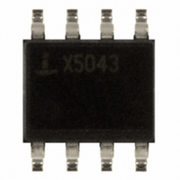
X5043S8 Intersil, X5043S8 Datasheet - Page 12

X5043S8
Manufacturer Part Number
X5043S8
Description
IC CPU SUPRV 4K EE RST LO 8SOIC
Manufacturer
Intersil
Type
Simple Reset/Power-On Resetr
Datasheet
1.X5043S8IZ-2.7A.pdf
(21 pages)
Specifications of X5043S8
Number Of Voltages Monitored
1
Output
Open Drain or Open Collector
Reset
Active Low
Reset Timeout
100 ms Minimum
Voltage - Threshold
4.38V
Operating Temperature
0°C ~ 70°C
Mounting Type
Surface Mount
Package / Case
8-SOIC (3.9mm Width)
Lead Free Status / RoHS Status
Contains lead / RoHS non-compliant
Available stocks
Company
Part Number
Manufacturer
Quantity
Price
Company:
Part Number:
X5043S8
Manufacturer:
INTERSIL
Quantity:
11 333
Company:
Part Number:
X5043S8-2.7
Manufacturer:
INTERSIL
Quantity:
14 101
Part Number:
X5043S8-2.7A
Manufacturer:
XICOR
Quantity:
20 000
Part Number:
X5043S8-2.7T1
Manufacturer:
INTERSIL
Quantity:
20 000
Company:
Part Number:
X5043S8-4.5
Manufacturer:
INTERSIL
Quantity:
12 488
Company:
Part Number:
X5043S8I-2.7
Manufacturer:
NEC
Quantity:
6 224
Company:
Part Number:
X5043S8I-2.7A
Manufacturer:
Intersil
Quantity:
1
Part Number:
X5043S8I-4.5A
Manufacturer:
INTERSIL
Quantity:
20 000
Part Number:
X5043S8IZ
Manufacturer:
INTERSIL
Quantity:
20 000
Part Number:
X5043S8IZ-2.7
Manufacturer:
INTERSIL
Quantity:
20 000
Operational Notes
The device powers-up in the following state:
Data Protection
The following circuitry has been included to prevent
inadvertent writes:
• A WREN instruction must be issued to set the Write
• CS must come HIGH at the proper clock count in order to
• Block Protect bits provide additional level of write
• The WP pin LOW blocks nonvolatile write operations.
1. The device is in the low power standby state.
2. A HIGH to LOW transition on CS is required to enter an
3. SO pin is high impedance.
4. The Write Enable Latch is reset.
5. The Flag Bit is reset.
6. Reset Signal is active for t
Enable Latch.
start a nonvolatile write cycle.
protection for the memory array.
active state and receive an instruction.
SCK
SCK
CS
CS
SI
SI
24 25 26 27 28 29 30 31
7
6
0
5
12
Data Byte 2
PURST
1
Instruction
4
2
.
3
3
2
4
8
1
9
FIGURE 9. WRITE MEMORY SEQUENCE
5
th
0
Bit of Address
6
32 33 34 35 36 37 38 39
7
7
6
X5043, X5045
8
7
5
Data Byte 3
6
9
4
8 Bit Address
10
5
3
2
12 13 14 15 16 17 18 19 20 21 22 23
3
1
2
0
1
0
6
7
5
6
Data Byte N
4
5
3
Data Byte 1
4
2
3
1
2
0
1
0
March 16, 2006
FN8126.2


