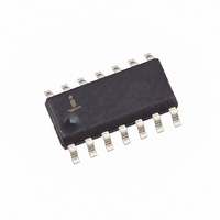
X5643S14I-2.7 Intersil, X5643S14I-2.7 Datasheet

X5643S14I-2.7
Specifications of X5643S14I-2.7
Related parts for X5643S14I-2.7
X5643S14I-2.7 Summary of contents
Page 1
... X25643, X25645) FN8135.1 detection circuitry protects the CC falls below the minimum thresholds are available, however, TRIP RESET/RESET Reset & X5643 = RESET X5645 = RESET Reset Intersil (and design registered trademark of Intersil Americas Inc. Copyright Intersil Americas Inc. 2005. All Rights Reserved CC returns ...
Page 2
PIN CONFIGURATION 8-Lead PDIP 1 8 CS/WDI X5643/ Pin Pin Pin PDIP SOIC TSSOP Name 1 2 & CS/WDI ...
Page 3
PRINCIPLES OF OPERATION Power-on Reset Application of power to the X5643/X5645 activates a power-on reset circuit. This circuit goes active at about 1V and pulls the RESET/RESET pin active. This signal prevents the system microprocessor from starting to operate with ...
Page 4
Figure 3. V Programming Sequence Flow Chart TRIP New V Applied = CC Old V Applied + Error CC Error ≥ Emax Emax = Maximum Desired Error 4 X5643, X5645 V Programming TRIP Execute Reset V TRIP Sequence Set V ...
Page 5
... Serial Peripheral Interface (SPI) and soft- ware protocol allowing operation on a simple four-wire bus. The device utilizes Intersil’s proprietary Direct Write cell, providing a minimum endurance of 100,000 cycles and a minimum data retention of 100 years. The device is designed to interface directly with the synchronous Serial Peripheral Interface (SPI) of many popular microcontroller families ...
Page 6
Table 2. Block Protect Matrix WREN CMD Status Register WEL WPEN The Write Enable Latch (WEL) bit indicates the sta- tus of the write enable latch. When WEL = 1, the latch ...
Page 7
Figure 5. Read EEPROM Array Sequence SCK Instruction SI High Impedance SO Setting the WP pin LOW while WPEN is a “1” while an internal write cycle to the status register is in progress will ...
Page 8
While the write is in progress following a status register or EEPROM sequence, the status register may be read to check the WIP bit. During this time the WIP bit will be high. OPERATIONAL NOTES The device powers-up in the ...
Page 9
Figure 8. Write Sequence SCK Instruction SCK Data Byte Figure 9. Status Register Write Sequence CS 0 ...
Page 10
ABSOLUTE MAXIMUM RATINGS Temperature under bias .................... -65°C to +135°C Storage temperature ......................... -65°C to +150°C Voltage on any pin with respect to V D.C. output current ............................................... 5mA Lead temperature (soldering, 10 seconds)........ 300°C RECOMMENDED OPERATING CONDITIONS Temperature Min. ...
Page 11
CAPACITANCE T = +25° 1MHz Symbol (2) C Output Capacitance (SO, RESET/RESET) OUT (2) C Input Capacitance (SCK, SI, CS, WP) IN Notes: (1) V min. and V max. are for reference only and are not ...
Page 12
Serial Input Timing CS t LEAD SCK MSB IN High Impedance SO Serial Output Timing Symbol f Clock frequency SCK t Output disable time DIS t Output valid from clock low V t Output hold time HO ...
Page 13
Power-Up and Power-Down Timing V CC RESET (X5643) RESET (X5645) RESET Output Timing Symbol V Reset trip point voltage, X5643-4.5A, X5643-4.5A TRIP Reset trip point voltage, X5643, X5645 Reset trip point voltage, X5643-2.7A, X5645-2.7A Reset trip point voltage, X5643-2.7, X5645-2.7 ...
Page 14
RESET/RESET Output Timing Symbol Parameter t Watchdog time out period, WDO WD1 = 1, WD0 = 0 WD1 = 0, WD0 = 1 WD1 = 0, WD0 = pulse width to reset the watchdog CST t Reset ...
Page 15
V Programming Specifications V TRIP Parameter t SCK V program voltage setup time VPS TRIP t SCK V program voltage hold time VPH TRIP t V program pulse width P TRIP t V level setup time TSU TRIP t V ...
Page 16
TYPICAL PERFORMANCE V Supply Current vs. Temperature ( Watchdog Timer Watchdog Timer Watchdog Timer Off ( -40 25 Temp (°C) V vs. Temperature ...
Page 17
PACKAGING INFORMATION Half Shoulder Width On All End Pins Optional .073 (1.84) Typ. 0.010 (0.25) NOTE: 1. ALL DIMENSIONS IN INCHES (IN PARENTHESES IN MILLIMETERS) 2. PACKAGE DIMENSIONS EXCLUDE MOLDING FLASH 17 X5643, X5645 8-Lead Plastic Dual In-Line Package Type ...
Page 18
PACKAGING INFORMATION 14-Lead Plastic Small Outline Gullwing Package Type S Pin 1 Index Pin 1 0.014 (0.35) 0.020 (0.51) (4X) 7° 0.050 (1.27) 0.010 (0.25) 0.020 (0.50) 0° - 8° 0.016 (0.410) 0.037 (0.937) NOTE: ALL DIMENSIONS IN INCHES (IN ...
Page 19
... X5643P-4.5A 0-70°C X5643S14-4.5A -40-85°C X5643S14I-4.5A 0-70°C 0-70°C X5643S14 -40-85°C X5643S14I 0-70°C X5643S14-2.7A 0-70°C X5643S14-2 8-Lead PDIP S14 = 14 Lead SOIC Blank = 5V ±10%, 0°C to +70° 5V±10%, 0°C to +70°C, V TRIP ±10%, -40°C to +85°C, V TRIP ± ...


