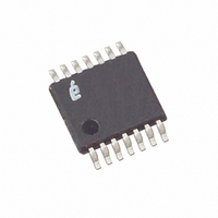
X40626V14-2.7A Intersil, X40626V14-2.7A Datasheet - Page 9

X40626V14-2.7A
Manufacturer Part Number
X40626V14-2.7A
Description
IC SUPERVISOR CPU DUAL 14-TSSOP
Manufacturer
Intersil
Type
Multi-Voltage Supervisorr
Datasheet
1.X40626S14.pdf
(22 pages)
Specifications of X40626V14-2.7A
Number Of Voltages Monitored
2
Output
Open Drain or Open Collector
Reset
Active Low
Reset Timeout
100 ms Minimum
Voltage - Threshold
2.23V, 2.93V
Operating Temperature
0°C ~ 70°C
Mounting Type
Surface Mount
Package / Case
14-TSSOP
Lead Free Status / RoHS Status
Contains lead / RoHS non-compliant
Figure 7. Acknowledge Response From Receiver
Serial Write Operations
Byte Write
For a write operation, the device requires the Slave
Address Byte and a Word Address Byte. This gives the
master access to any one of the words in the array. After
receipt of the Word Address Byte, the device responds
with an acknowledge, and awaits the next eight bits of
Figure 8. Byte Write Sequence
A write to a protected block of memory will suppress
the acknowledge bit.
Page Write
The device is capable of a page write operation. It is
initiated in the same manner as the byte write opera-
tion; but instead of terminating the write cycle after the
first data byte is transferred, the master can transmit
an unlimited number of 8-bit bytes. After the receipt of
each byte, the device will respond with an acknowl-
edge, and the address is internally incremented by
one. The page address remains constant. When the
from Receiver
Data Output
Data Output
SCL from
Signals from
Signals from
the Master
Master
the Slave
SDA Bus
from
9
Start
S
A
R
T
T
S
1 0 1 0 0
Address
Slave
S
1
S
0
1
0
A
C
K
Word Address
Byte 1
X40626
data. After receiving the 8 bits of the Data Byte, the
device again responds with an acknowledge. The master
then terminates the transfer by generating a stop condi-
tion, at which time the device begins the internal write
cycle to the nonvolatile memory. During this internal write
cycle, the device inputs are disabled, so the device will
not respond to any requests from the master. The SDA
output is at high impedance. See Figure 8.
counter reaches the end of the page, it “rolls over” and
goes back to ‘0’ on the same page. This means that
the master can write 64 bytes to the page starting at
any location on that page. If the master begins writing
at location 60, and loads 12 bytes, then the first 4
bytes are written to locations 60 through 63, and the
last 8 bytes are written to locations 0 through 7. After-
wards, the address counter would point to location 8 of
the page that was just written. If the master supplies
more than 64 bytes of data, then new data over-writes
the previous data, one byte at a time.
A
C
K
Word Address
Byte 0
8
A
C
K
Acknowledge
Data
9
A
C
K
S
O
P
P
T
March 28, 2005
FN8119.0


