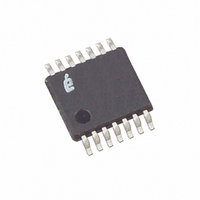
X40626V14-2.7AT1 Intersil, X40626V14-2.7AT1 Datasheet - Page 12

X40626V14-2.7AT1
Manufacturer Part Number
X40626V14-2.7AT1
Description
IC SUPERVISOR CPU DUAL 14-TSSOP
Manufacturer
Intersil
Type
Multi-Voltage Supervisorr
Datasheet
1.X40626S14.pdf
(22 pages)
Specifications of X40626V14-2.7AT1
Number Of Voltages Monitored
2
Output
Open Drain or Open Collector
Reset
Active Low
Reset Timeout
100 ms Minimum
Voltage - Threshold
2.23V, 2.93V
Operating Temperature
0°C ~ 70°C
Mounting Type
Surface Mount
Package / Case
14-TSSOP
Lead Free Status / RoHS Status
Contains lead / RoHS non-compliant
Random Read
Random read operation allows the master to access
any memory location in the array. Prior to issuing the
Slave Address Byte with the R/W bit set to one, the
master must first perform a “dummy” write operation.
The master issues the start condition and the Slave
Address Byte, receives an acknowledge, then issues
the Word Address Bytes. After acknowledging receipts
Figure 13. Random Address Read Sequence
There is a similar operation, called “Set Current
Address” where the device does no operation, but
enters a new address into the address counter if a
stop is issued instead of the second start shown in Fig-
ure 13. The device goes into standby mode after the
stop and all bus activity will be ignored until a start is
detected. The next Current Address Read operation
reads from the newly loaded address. This operation
could be useful if the master knows the next address it
needs to read, but is not ready for the data.
Sequential Read
Sequential reads can be initiated as either a current
address read or random address read. The first Data
Byte is transmitted as with the other modes; however,
the master now responds with an acknowledge, indicat-
ing it requires additional data. The device continues to
output data for each acknowledge received. The master
terminates the read operation by not responding with an
acknowledge and then issuing a stop condition.
Signals from
Signals from
the Master
SDA Bus
the Slave
R
S
T
A
T
S
1 0 1 0
12
Address
Slave
0
S
1
S
0
0
A
C
K
Word Address
Byte 1
X40626
A
C
K
Word Address
Byte 0
of the Word Address Bytes, the master immediately
issues another start condition and the Slave Address
Byte with the R/W bit set to one. This is followed by an
acknowledge from the device and then by the eight bit
word. The master terminates the read operation by not
responding with an acknowledge and then issuing a
stop condition. Refer to Figure 13 for the address,
acknowledge, and data transfer sequence.
The data output is sequential, with the data from address
n followed by the data from address n + 1. The address
counter for read operations increments through all page
and column addresses, allowing the entire memory con-
tents to be serially read during one operation. At the end
of the address space the counter “rolls over” to address
0000H and the device continues to output data for each
acknowledge received. Refer to Figure 14 for the
acknowledge and data transfer sequence.
A
C
K
S
R
S
T
A
T
1 0 1 0
Address
Slave
0
S
1
S
0
1
A
C
K
Data
O
P
S
P
T
March 28, 2005
FN8119.0


