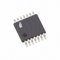
X40626V14-4.5AT1 Intersil, X40626V14-4.5AT1 Datasheet - Page 7

X40626V14-4.5AT1
Manufacturer Part Number
X40626V14-4.5AT1
Description
IC SUPERVISOR CPU DUAL 14-TSSOP
Manufacturer
Intersil
Type
Multi-Voltage Supervisorr
Datasheet
1.X40626S14.pdf
(22 pages)
Specifications of X40626V14-4.5AT1
Number Of Voltages Monitored
2
Output
Open Drain or Open Collector
Reset
Active Low
Reset Timeout
100 ms Minimum
Voltage - Threshold
2.93V, 4.63V
Operating Temperature
0°C ~ 70°C
Mounting Type
Surface Mount
Package / Case
14-TSSOP
Lead Free Status / RoHS Status
Contains lead / RoHS non-compliant
Available stocks
Company
Part Number
Manufacturer
Quantity
Price
Company:
Part Number:
X40626V14-4.5AT1
Manufacturer:
VISHAY
Quantity:
3 123
Table 1. Write Protect Enable Bit and WP Pin Function
Writing to the Control Register
Changing any of the nonvolatile bits of the control reg-
ister requires the following steps:
– Write a 02H to the Control Register to set the Write
– Write a 06H to the Control Register to set both the
– Write a value to the Control Register that has all the
– A read operation occurring between any of the previ-
Enable Latch (WEL). This is a volatile operation, so
there is no delay after the write. (Operation pro-
ceeded by a start and ended with a stop).
Register Write Enable Latch (RWEL) and the WEL
bit. This is also a volatile cycle. The zeros in the data
byte are required. (Operation proceeded by a start
and ended with a stop).
control bits set to the desired state. This can be rep-
resented as 0xys t01r in binary, where xy are the
WD bits, and rst are the BP bits. (Operation pre-
ceeded by a start and ended with a stop). Since this
is a nonvolatile write cycle it will take up to 10ms to
complete. The RWEL bit is reset by this cycle and
the sequence must be repeated to change the non-
volatile bits again. If bit 2 is set to ‘1’ in this third step
(0xys t11r) then the RWEL bit is set, but the WD1,
WD0, BP2, BP1 and BP0 bits remain unchanged.
Writing a second byte to the control register is not
allowed. Doing so aborts the write operation and
returns a NACK.
ous operations will not interrupt the register write
operation.
HIGH
HIGH
LOW
WP
WPEN
X
0
1
Memory Array not
Block Protected
7
Writes OK
Writes OK
Writes OK
Block Protected
Memory Array
Writes Blocked
Writes Blocked
Writes Blocked
X40626
– The RWEL bit cannot be reset without writing to the
To illustrate, a sequence of writes to the device con-
sisting of [02H, 06H, 02H] will reset all of the nonvola-
tile bits in the Control Register to 0. A sequence of
[02H, 06H, 06H] will leave the nonvolatile bits
unchanged and the RWEL bit remains set.
SERIAL INTERFACE
Serial Interface Conventions
The device supports a bidirectional bus oriented proto-
col. The protocol defines any device that sends data
onto the bus as a transmitter, and the receiving device
as the receiver. The device controlling the transfer is
called the master and the device being controlled is
called the slave. The master always initiates data
transfers, and provides the clock for both transmit and
receive operations. Therefore, the devices in this fam-
ily operate as slaves in all applications.
Serial Clock and Data
Data states on the SDA line can change only during
SCL LOW. SDA state changes during SCL HIGH are
reserved for indicating start and stop conditions. See
Figure 5.
nonvolatile control bits in the control register, power
cycling the device or attempting a write to a write
protected block.
Block Protect
Writes Blocked
Writes OK
Writes OK
Bits
Writes Blocked
WPEN Bit
Writes OK
Writes OK
Protection
Hardware
Software
Software
March 28, 2005
FN8119.0


