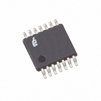
X5163V14I-2.7T1 Intersil, X5163V14I-2.7T1 Datasheet

X5163V14I-2.7T1
Specifications of X5163V14I-2.7T1
Related parts for X5163V14I-2.7T1
X5163V14I-2.7T1 Summary of contents
Page 1
... All other trademarks mentioned are the property of their respective owners. X5163, X5165 June 1, 2006 FN8128.3 detection and reset assertion reset threshold voltage using protection 14 Ld TSSOP X5163, X5165 RESET/RESET SCK Intersil (and design registered trademark of Intersil Americas Inc. Copyright Intersil Americas Inc. 2005, 2006. All Rights Reserved ...
Page 2
... X5165S8I-2.7* X5163S8IZ-2.7* X5163 Z G X5165S8IZ-2.7* (Note) (Note) X5163V14-2.7* X5163V F X5165V14-2.7* X5163V14Z-2.7* X5163V Z F X5165V14Z-2.7* (Note) (Note) X5163V14I-2.7* X5163V G X5165V14I-2.7* X5163V14IZ-2.7* X5163V Z G X5165V14IZ-2.7* (Note) (Note) X5163P-2.7A X5163P AN X5165P-2.7A X5163PZ-2.7A X5163P Z AN X5165PZ-2.7A (Note) (Note) X5163PI-2.7A X5163P AP X5165PI-2.7A X5163PIZ-2.7A X5163P Z AP X5165PIZ-2.7A ...
Page 3
... X5163V Z AL X5165V14Z-4.5A (Note) (Note) X5163V14I-4.5A X5163V AM X5165V14I-4.5A X5163V14IZ-4.5A X5163V Z AM X5165V14IZ-4.5A (Note) (Note) *Add "T1" suffix for tape and reel. **Pb-free PDIPs can be used for through hole wave solder processing only. They are not intended for use in Reflow solder processing applications. ...
Page 4
Block Diagram WP SI Data Register SO Command SCK Decode & Control CS/WDI Logic V Threshold CC Reset Logic V CC Pin Description PIN (SOIC/PDIP) PIN TSSOP NAME 1 1 CS/WDI ...
Page 5
Principles Of Operation Power-on Reset Application of power to the X5163, X5165 activates a Power- on Reset Circuit. This circuit goes active at 1V and pulls the RESET/RESET pin active. This signal prevents the system microprocessor from starting to operate ...
Page 6
NEW V APPLIED = CC OLD V APPLIED + ERROR CC ERROR > -EMAX EMAX = MAXIMUM DESIRED ERROR FIGURE 3. V 4.7K V TRIP + ADJ. PROGRAM 6 X5163, X5165 V PROGRAMMING TRIP EXECUTE RESET V TRIP SEQUENCE SET ...
Page 7
... SPI Serial Memory The memory portion of the device is a CMOS Serial EEPROM array with Intersil’s block lock protection. The array is internally organized The device features a Serial Peripheral Interface (SPI) and software protocol allowing operation on a simple four-wire bus. The device utilizes Intersil’s proprietary Direct Write providing a minimum endurance of 100,000 cycles and a minimum data retention of 100 years ...
Page 8
The Write Enable Latch (WEL) bit indicates the Status of the Write Enable Latch. When WEL = 1, the latch is set HIGH and when WEL = 0 the latch is reset LOW. The WEL bit is a volatile, read ...
Page 9
When WP is HIGH, all functions, including nonvolatile writes to the Status Register operate normally. Setting the WPEN bit in the Status Register to “0” blocks the WP pin function, allowing writes to the Status Register when WP is HIGH ...
Page 10
SCK INSTRUCTION SI HIGH IMPEDANCE SO FIGURE 6. READ STATUS REGISTER SEQUENCE CS SCK SI HIGH IMPEDANCE SO FIGURE 7. WRITE ENABLE LATCH SEQUENCE SCK INSTRUCTION ...
Page 11
CS 0 SCK SI HIGH IMPEDANCE SO Symbol Table WAVEFORM INPUTS OUTPUTS MUST BE WILL BE STEADY STEADY MAY CHANGE WILL CHANGE FROM LOW TO FROM LOW TO HIGH HIGH MAY CHANGE WILL CHANGE FROM HIGH TO FROM HIGH TO ...
Page 12
Absolute Maximum Ratings Temperature under bias . . . . . . . . . . . . . . . . . . . . . . . .-65 to +135°C Storage temperature . . . . . . ...
Page 13
OUTPUT RESET/RESET 1.64kΩ 100pF FIGURE 10. EQUIVALENT A.C. LOAD CIRCUIT Electrical Specifications Serial Input Timing SYMBOL f Clock Frequency SCK t Cycle Time CYC t CS Lead Time LEAD t CS Lag Time LAG ...
Page 14
AC Electrical Specifications Serial Output Timing SYMBOL f Clock Frequency SCK t Output Disable Time DIS t Output Valid from Clock Low V t Output Hold Time HO (3) t Output Rise Time RO (3) t Output Fall Time FO ...
Page 15
RESET Output Timing SYMBOL V Reset Trip Point Voltage, X5163-4.5A, X5163-4.5A TRIP Reset Trip Point Voltage, X5163, X5165 Reset Trip Point Voltage, X5163-2.7A, X5165-2.7A Reset Trip Point Voltage, X5163-2.7, X5165-2 Hysteresis (HIGH to LOW vs. LOW to HIGH ...
Page 16
TRIP t VPS SCK FIGURE 13 TRIP VPS SCK FIGURE 14 X5163, X5165 t THD t TSU ...
Page 17
V Programming Specifications: V TRIP PARAMETER t SCK V Program Voltage Setup time VPS TRIP t SCK V Program Voltage Hold time VPH TRIP t V Program Pulse Width P TRIP t V Level Setup time TSU TRIP t V ...
Page 18
WATCHDOG TIMER WATCHDOG TIMER WATCHDOG TIMER OFF ( -40 25 TEMP (°C) FIGURE 15. V SUPPLY CURRENT VS. TEMPERATURE (I CC 5.025 5.000 4.975 ...
Page 19
Small Outline Package Family (SO PIN #1 I.D. MARK 0.010 SEATING PLANE 0.004 C 0.010 MDP0027 SMALL OUTLINE PACKAGE FAMILY (SO) SYMBOL SO-8 SO-14 ...
Page 20
Plastic Dual-In-Line Packages (PDIP) D SEATING PLANE MDP0031 PLASTIC DUAL-IN-LINE PACKAGE SYMBOL PDIP8 PDIP14 A 0.210 0.210 A1 0.015 0.015 A2 0.130 0.130 b 0.018 0.018 b2 0.060 0.060 c 0.010 0.010 D 0.375 0.750 E 0.310 ...
Page 21
... Accordingly, the reader is cautioned to verify that data sheets are current before placing orders. Information furnished by Intersil is believed to be accurate and reliable. However, no responsibility is assumed by Intersil or its subsidiaries for its use; nor for any infringements of patents or other rights of third parties which may result from its use ...


