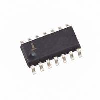
X5648S14IT1 Intersil, X5648S14IT1 Datasheet - Page 7

X5648S14IT1
Manufacturer Part Number
X5648S14IT1
Description
IC SUPERVISOR CPU 64K EE 14-SOIC
Manufacturer
Intersil
Type
Simple Reset/Power-On Resetr
Datasheet
1.X5648P.pdf
(18 pages)
Specifications of X5648S14IT1
Number Of Voltages Monitored
1
Output
Open Drain or Open Collector
Reset
Active Low
Reset Timeout
100 ms Minimum
Voltage - Threshold
4.38V
Operating Temperature
-40°C ~ 85°C
Mounting Type
Surface Mount
Package / Case
14-SOIC (3.9mm Width), 14-SOL
Lead Free Status / RoHS Status
Contains lead / RoHS non-compliant
Figure 5. Read EEPROM Array Sequence
Write Sequence
Prior to any attempt to write data into the device, the
Write Enable Latch (WEL) must first be set by issuing
the WREN instruction (Figure 3). CS is first taken LOW,
then the WREN instruction is clocked into the device.
After all eight bits of the instruction are transmitted, CS
must then be taken HIGH. If the user continues the
write operation without taking CS HIGH after issuing the
WREN instruction, the write operation will be ignored.
To write data to the EEPROM memory array, the user
then issues the WRITE instruction followed by the 16
bit address and then the data to be written. Any
unused address bits are specified to be “0’s”. The
WRITE operation minimally takes 32 clocks. CS must
go low and remain low for the duration of the opera-
tion. If the address counter reaches the end of a page
and the clock continues, the counter will roll back to
the first address of the page and overwrite any data
that may have been previously written.
For the page write operation (byte or page write) to be
completed, CS can only be brought HIGH after bit 0 of
the last data byte to be written is clocked in. If it is
brought HIGH at any other time, the write operation
will not be completed (Figure 4).
To write to the status register, the WRSR instruction is
followed by the data to be written (Figure 5). Data bits
0 and 1 must be “0”.
While the write is in progress following a status regis-
ter or EEPROM sequence, the status register may be
read to check the WIP bit. During this time the WIP bit
will be high.
SCK
SO
CS
SI
High Impedance
0
1
Instruction
7
2
3
4
5
6
7
15 14 13
8
X5648, X5649
9
16 Bit Address
10
OPERATIONAL NOTES
The device powers-up in the following state:
– The device is in the low power standby state.
– A HIGH to LOW transition on CS is required to enter
– SO pin is high impedance.
– The write enable latch is reset.
– The flag bit is reset.
– Reset signal is active for t
Data Protection
The following circuitry has been included to prevent
inadvertent writes:
– A WREN instruction must be issued to set the write
– CS must come HIGH at the proper clock count in
20 21 22 23 24 25 26 27 28 29 30
3
an active state and receive an instruction.
enable latch.
order to start a nonvolatile write cycle.
2
1
0
MSB
7
6
5
Data Out
4
PURST
3
.
2
1
0
March 17, 2005
FN8136.0


